Patent application title: ELECTRIC CONTACT STRUCTURE FOR LIGHT EMITTING DIODES
Inventors:
Wei-Chun Tseng (Taichung City, TW)
Wei-Yu Yen (Taichung City, TW)
Wei-Yu Yen (Taichung City, TW)
Fu-Bang Chen (Taichung City, TW)
Fu-Bang Chen (Taichung City, TW)
Chih-Sung Chang (Taichung City, TW)
Chih-Sung Chang (Taichung City, TW)
IPC8 Class:
USPC Class:
257 99
Class name: Active solid-state devices (e.g., transistors, solid-state diodes) incoherent light emitter structure with housing or contact structure
Publication date: 2013-11-07
Patent application number: 20130292734
Abstract:
An electric contact structure adopted for an LED comprises a nitride
middle layer and an N-type metal electrode layer. The LED includes an
N-type semiconductor layer, a light emission layer and a P-type
semiconductor layer that are stacked to form a sandwich structure. The
nitride middle layer is patterned and formed on the N-type semiconductor
layer. The N-type metal electrode layer is formed on the nitride middle
layer and prevented from being damaged by diffusion of the metal ions as
the nitride middle layer serves as a blocking interface, thus electric
property of the N-type semiconductor layer can be maintained stable. The
nitride middle layer would not be softened and condensed due to long-term
high temperature, thereby is enhanced adhesion. Moreover, the N-type
metal electrode layer further can be prevented from peeling off, hence is
increased the lifespan of the LED.Claims:
1. An electric contact structure for a light emitting diode which
includes an N-type semiconductor layer, a light emission layer and a
P-type semiconductor layer that are stacked to form a sandwich structure,
comprising: a nitride middle layer patterned and formed on the N-type
semiconductor layer; and an N-type metal electrode layer formed on the
nitride middle layer.
2. The electric contact structure of claim 1, wherein the nitride middle layer is selected from the group consisting of aluminum nitride (AlN), titanium nitride (TiN) and chromium nitride (CrN).
3. The electric contact structure of claim 2, wherein composition ratio of nitrogen and aluminum in the aluminum nitride (AlN) is X:1-X, where X is between 0.05 and 0.15, wherein composition ratio of nitrogen and titanium in the titanium nitride (TiN) is X:1-X, where X is between 0.05 and 0.15, and wherein composition ratio of nitrogen and chromium in the chromium nitride (CrN) is X:1-X, where X is between 0.05 and 0.15.
4. The electric contact structure of claim 2, wherein the nitride middle layer is formed at a thickness between 10 nanometers and 500 nanometers.
5. The electric contact structure of claim 1, wherein the N-type metal electrode layer is selected from the group consisting of aluminum, titanium, nickel, chromium, platinum and gold.
6. The electric contact structure of claim 5, wherein the N-type metal electrode layer is formed at a thickness greater than 1 μm.
7. The electric contact structure of claim 5, wherein the N-type metal electrode layer includes at least two types of materials that are interlaced and stacked.
8. The electric contact structure of claim 1, wherein the N-type semiconductor layer includes an irregular surface, and the nitride middle layer and the N-type metal electrode layer are formed on the irregular surface.
9. The electric contact structure of claim 8, wherein the irregular surface is a continuous serrated surface.
10. The electric contact structure of claim 9, wherein the irregular surface includes a peak to peak distance greater than 500 nanometers.
11. The electric contact structure of claim 1, wherein the N-type semiconductor layer includes an irregular surface where no nitride middle layer is formed.
Description:
FIELD OF THE INVENTION
[0001] The present invention relates to a light emitting diode (LED) and particularly to an electric contact structure for LEDs.
BACKGROUND OF THE INVENTION
[0002] Light emitting diode (LED) mainly includes multiple layers of semiconductor materials formed by epitaxy. Take a blue LED as an example, it mainly formed by III-nitride based epitaxial films.
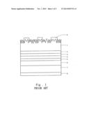
[0003] Please refer to FIG. 1 for a conventional vertical LED. It comprise an N-type semiconductor layer 1, a light emission layer 2 and a P-type semiconductor layer 3, and under the P-type semiconductor layer 3 in this order a mirror layer 4, a buffer layer 5, a bonding layer 6, a silicon substrate 7 and a P-type electrode 8. The surface of the N-type semiconductor layer 1 can be treated in a coarse process to enhance light extraction efficiency. The LED also can have an N-type electrode 9 located thereon. When a voltage is applied to the N-type electrode 9 and P-type electrode 8, the N-type semiconductor layer 1 provides electrons, and the P-type semiconductor layer 3 provides electric holes, then the electrons and electric holes are joined in the light emission layer 2 to generate light.
[0004] The N-type electrode 9 generally is made of metal, such as silver, aluminum, nickel or the like. The N-type electrode 9 is easily softened and condensed to become spherical shape due to high temperature and results in peeling off. After used for a period of time, metal ions slowly permeate into the N-type semiconductor layer 1 that causes unstable electric property and results in shortening lifespan of the LED. It still leaves a lot to be desired, especially in terms of durability.
SUMMARY OF THE INVENTION
[0005] The primary object of the present invention is to provide an electric contact structure for LEDs to enhance the lifespan thereof.
[0006] The electric contact structure according to the invention is adopted for an LED which comprises an N-type semiconductor layer, a light emission layer and a P-type semiconductor layer that are stacked to form a sandwich structure. The invention includes a nitride middle layer and an N-type metal electrode layer. The nitride middle layer is patterned and formed on the N-type semiconductor layer. The N-type metal electrode layer is formed on the nitride middle layer.
[0007] Through the nitride middle layer serving as a blocking interface, the N-type semiconductor layer can be protected by the blocking interface to be prevented from being damaged by diffusion of the metal ions, thereby electric property of the N-type semiconductor layer can be maintained stable. The nitride middle layer would not be softened and condensed to become spherical shape due to long-term high temperature, hence adhesion increases and the N-type metal electrode layer further can be prevented from peeling off. As a result, the lifespan of the LED increases.
[0008] The foregoing, as well as additional objects, features and advantages of the invention will be more readily apparent from the following detailed description, which proceeds with reference to the embodiments and accompanying drawings. The embodiments serve merely for illustrative purpose and are not the limitations of the invention.
BRIEF DESCRIPTION OF THE DRAWINGS
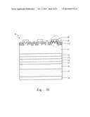
[0009] FIG. 1 is a schematic view of a conventional LED structure.
[0010] FIG. 2A is a schematic view of a first embodiment of the invention.
[0011] FIG. 2B is a fragmentary enlarged view according to FIG. 2A.
[0012] FIG. 3A is a schematic view of a second embodiment of the invention.
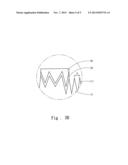
[0013] FIG. 3B is a fragmentary enlarged view according to FIG. 3A.
DETAILED DESCRIPTION OF THE PREFERRED EMBODIMENTS
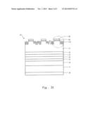
[0014] Please refer to FIGS. 2A and 2B for a first embodiment of the invention that is adopted for an LED 10 and includes a nitride middle layer 20 and an N-type metal electrode layer 30. The LED 10 comprises an N-type semiconductor layer 11, a light emission layer 12 and a P-type semiconductor layer 13 that are stacked to form a sandwich structure, and also has in this order under the P-type semiconductor layer 13, a mirror layer 14, a buffer layer 15, a bonding layer 16, a silicon substrate 17 and a P-type electrode 18.
[0015] The nitride middle layer 20 is patterned and formed on the N-type semiconductor layer 11, and can be selected from the group consisting of aluminum nitride (AlN), titanium nitride (TiN) and chromium nitride (CrN), i.e. the composition of the nitride middle layer 20 can be Ti(X)N(1-X), Al(X)N(1-X) or Cr(X)N(1-X), where 0.05<X<0.15.
[0016] In other words, the ratio of nitrogen and aluminum in the AlN is X:1-X, with the X between 0.05 and 0.15. Similarly, the ratio of nitrogen and titanium in TiN, and nitrogen and chromium in CrN also is X:1-X, with X between 0.05 and 0.15. The nitride middle layer 20 is preferably formed at a thickness between 10 nanometers and 500 nanometers. Since the nitride can maintain in a stable condition at high temperature to block diffusion of metal ions, the nitride middle layer 20 serves as a blocking interface to avoid the LED from aging rapidly. The area of the N-type semiconductor layer 11 without the nitride middle layer 20 has an irregular surface 111 to prevent total reflection and enhance light extraction efficiency. The irregular surface 111 can be formed through a physical method, such as plasma bombardment or the like.
[0017] The N-type metal electrode layer 30 is formed on the nitride middle layer 20, and can be selected from the group consisting of aluminum, titanium, nickel, chromium, platinum and gold, and is formed at a thickness greater than 1 μm. The N-type metal electrode layer 30 also includes at least two types of metal materials that are interlaced and stacked.
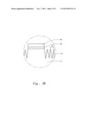
[0018] Please refer to FIGS. 3A and 3B for a second embodiment of the invention. In this embodiment, the N-type semiconductor layer 11 can have an irregular surface 111, and the nitride middle layer 20 and N-type metal electrode layer 30 are formed on the irregular surface 111 which can be a continuous serrated surface with a peak to peak distance D, preferably greater than 500 nanometers.
[0019] As a conclusion, as the nitride middle layer 20 of the invention is in contact with the N-type semiconductor layer to form Schottky contact, but the forward voltage would not be increased significantly, thus the nitride middle layer 20 can function as a blocking interface to block diffusion of metal ions to allow physical characteristics of the N-type semiconductor layer to be maintained stable at high temperature, so that the N-type semiconductor layer 11 can be prevented from being damaged by diffusion of the metal ions and its electric property also can be maintained stable. Moreover, the nitride middle layer 20 would not be softened and condensed to become a spherical shape due to high temperature, hence adhesion can be maintained and the N-type metal electrode layer 30 further can be prevented from peeling off. As a result, the lifespan of the LED can increase to meet use requirements.
User Contributions:
Comment about this patent or add new information about this topic:
Images included with this patent application:
 |  |
 |  |
 |  |
| New patent applications in this class: | |
| Date | Title |
|---|---|
| 2019-05-16 | Optoelectronic device and the manufacturing method thereof |
| 2019-05-16 | Light emitting element including metal bulk |
| 2019-05-16 | Ultraviolet light emitting diode |
| 2019-05-16 | Light-emitting device |
| 2018-01-25 | Display device and method of manufacturing the same |
| New patent applications from these inventors: | |
| Date | Title |
|---|---|
| 2016-03-03 | Semiconductor light-emitting device and fabricating method thereof |
| 2014-12-18 | Semiconductor light-emitting device and fabricating method thereof |
| Top Inventors for class "Active solid-state devices (e.g., transistors, solid-state diodes)" | |
| Rank | Inventor's name |
|---|---|
| 1 | Shunpei Yamazaki |
| 2 | Shunpei Yamazaki |
| 3 | Kangguo Cheng |
| 4 | Huilong Zhu |
| 5 | Chen-Hua Yu |