Patent application title: LIGHT EMITTING DIODE LIGHT SOURCE DEVICE
Inventors:
Chih-Peng Hsu (Hsinchu, TW)
Advanced Optoelectronic Technology, Inc.
Advanced Optoelectronic Technology, Inc.
Chung-Min Chang (Hsinchu, TW)
Chung-Min Chang (Hsinchu, TW)
Hsuen-Feng Hu (Hsinchu, TW)
Chien-Lin Chang-Chien (Hsinchu, TW)
Yu-Wei Tsai (Hsinchu, TW)
Assignees:
ADVANCED OPTOELECTRONIC TECHNOLOGY, INC.
IPC8 Class:
USPC Class:
257 98
Class name: Active solid-state devices (e.g., transistors, solid-state diodes) incoherent light emitter structure with reflector, opaque mask, or optical element (e.g., lens, optical fiber, index of refraction matching layer, luminescent material layer, filter) integral with device or device enclosure or package
Publication date: 2013-10-31
Patent application number: 20130285094
Abstract:
An LED light source device includes an LED light source, a first
translucent structure covering the LED light source and a second
translucent structure covering the first translucent structure. An
interior of the first translucent structure has light scattering powder
distributed therein. The LED light source is embedded in the first
translucent structure. The LED light source is covered by the light
scattering powder. The second translucent structure has a radius of R and
an index of refraction of N1 , while the first translucent structure
has a radius of r, wherein R, r and N1 satisfy the following
relation: N1<R/(2r-R).Claims:
1. An LED (light emitting diode) light source device, comprising: an LED
light source; a first translucent structure covering the LED light
source, powder with a characteristic of scattering light being
distributed in an interior of the first translucent structure, the LED
light source being embedded in the first translucent structure and
covered by the powder; and a second translucent structure covering the
first translucent structure.
2. The LED light source device of claim 1, wherein an outer contour of the first translucent structure and an outer contour of the second translucent structure are both partly spherical, the outer contour of the first translucent structure is coincident with a part of a first sphere, the outer contour of the second translucent structure is coincident with a part of a second sphere, and radiuses of the first sphere and the second sphere satisfy following condition: R>r, wherein r represents radius of the first sphere, R represents radius of the second sphere, and the first sphere for which the outer contour of the first translucent structure is partly coincidental is internally tangent with the second sphere for which the outer contour of the second translucent structure is partly coincidental.
3. The LED light source device of claim 2, wherein the LED light source is located on an extension line of a connecting line of the centers of the first translucent structure and the second translucent.
4. The LED light source device of claim 2, wherein the index of refraction of the second translucent structure satisfies following condition: N1<R/(2r-R), wherein N1 represents the index of refraction of the second translucent structure.
5. The LED light source device of claim 1, wherein the powder is made of phosphor materials.
6. The LED light source device of claim 1, wherein the powder is a mixture of phosphor materials and powder materials which include SiO2, Al2O3 or silicate.
7. The LED light source device of claim 1, wherein the powder is distributed in the interior of the whole first translucent structure evenly.
8. An LED light source device, comprising: an LED light source; a translucent structure located on a light path of the LED light source; powder filled in an interior of the translucent structure, the powder having a characteristic of scattering light; and wherein the LED light source is embedded in the translucent structure.
9. The LED light source device of claim 7, wherein an outer contour of the translucent structure and an outer contour of the powder are both partly spherical, and the outer contour of the powder is coincident with a part of a first sphere, the outer contour of the translucent structure is coincident with a part of a second sphere, and radiuses of the first sphere and the second sphere satisfy following condition: R>r, wherein r represents radius of the first sphere, R represents radius of the second sphere, and the first sphere for which the outer contour of the powder is partly coincidental is internally tangent with the second sphere for which the outer contour of the translucent structure is partly coincidental.
10. The LED light source device of claim 9, wherein the index of refraction of the translucent structure satisfies following condition: N1<R/(2r-R), wherein N1 represents the index of refraction of the translucent structure.
11. The LED light source device of claim 8, wherein the LED light source is located on an extension line of a connecting line of the centers of the translucent structure and the powder.
12. The LED light source device of claim 8, wherein the powder is made of phosphor materials.
13. The LED light source device of claim 8, wherein the powder is a mixture of phosphor materials and powder materials which include SiO2, Al2O3 or silicate.
Description:
BACKGROUND
[0001] 1. Technical Field
[0002] The present disclosure relates to an LED (light emitting diode) light source device, and more particularly to an LED light source device having a uniform light distribution and a large viewing angle.
[0003] 2. Description of Related Art
[0004] LEDs have been widely promoted as light sources of electronic devices owing to many advantages, such as high luminosity, low operational voltage and low power consumption. However, as a point light source, a viewing angle of the LED is only about 120°, and a light field of the LED is not uniform.
[0005] Therefore, an LED light source device capable of overcoming the above described shortcomings is desired.
BRIEF DESCRIPTION OF THE DRAWINGS
[0006] Many aspects of the present disclosure can be better understood with reference to the following drawings. The components in the drawings are not necessarily drawn to scale, the emphasis instead being placed upon clearly illustrating the principles of the present disclosure. Moreover, in the drawings, like reference numerals designate corresponding parts throughout the several views.
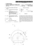
[0007] FIG. 1 shows a schematic view of an LED light source device in accordance with an embodiment of the present disclosure.
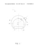
[0008] FIG. 2 shows a geometric diagram of a first translucent structure and a second translucent structure of the LED light source device illustrated in FIG. 1 of the present disclosure.
DETAILED DESCRIPTION
[0009] Referring to FIG. 1, an LED light source device 1 in accordance with an exemplary embodiment of the present disclosure includes an LED light source 10, a first translucent structure 20 covering the LED light source 10, and a second translucent structure 30 covering the first translucent structure 20.
[0010] In this embodiment, the LED light source 10 is an LED package, and includes a bottom surface 11. The LED light source 10 can also be an LED chip.
[0011] The first translucent structure 20 is located on a light path of the LED light source 10, and a kind of powder 21 with a characteristic of scattering light is distributed in an interior of the whole first translucent structure 20 evenly. Referring to FIG. 2, in this embodiment, the first translucent structure 20 is partly spherical. The LED light source 10 is embedded in the first translucent structure 20, merely with the bottom surface 11 exposed outside and coplanar with a bottom edge of the first translucent structure 20. Alternatively, the LED light source 10 can also be located outside of the first translucent structure 20, and the powder 21 can also be merely coated at an outer surface of the first translucent structure 20.
[0012] The second translucent structure 30 covers the first translucent structure 20 therebelow, and attaches to an outer surface of the first translucent structure 20. In this embodiment, the second translucent structure 30 is a lens, and the outer contour of the second translucent structure 30 is partly spherical. The first translucent structure 20 is embedded in the second translucent structure 30, and the bottom surface 11 of the LED light source 10 is coplanar with a bottom edge the second translucent structure 30. The index of refraction of the second translucent structure 30 is represented by N1.
[0013] Referring to FIG. 2, it shows a geometric diagram of the first translucent structure 20 and the second translucent structure 30. Sphere M and sphere N are defined, and the centers and radius of the sphere M and sphere N are illustrated and represented by point O2, point O1, r and R, respectively, and R>r. The sphere M is internally tangent with the sphere N at a point C. An outer contour of the first translucent structure 20 is coincident with a part of the sphere M, and an outer contour of the second translucent structure 30 is coincident with a part of the sphere N. The point C is located on an extension line of O1 O2 and away from the point O1. The extension line of O1 O2 and the sphere M intersect at a point A. The LED light source 10 is located on the extension line of O1 O2 , and above the point C.
[0014] During operation of the LED light source 10, the light emitted from the LED light source 10 travels toward the first translucent structure 20. Under light scattering of the powder 21, the light output by the first translucent structure 20 will enter the second transparent structure 30 along various travelling directions. Therefore, the viewing angle of the LED light source device 1 is increased, and the light field of the LED light source device 1 is modified to be uniform. When light travelling from the point A to a point B on the outer contour of the second translucent structure 30, along a direction perpendicular to the line O1 O2 , strikes onto the outer contour of the second translucent structure 30, an incident angle thereof is defined as θ. A critical angle of total reflection of the outer contour of the second translucent structure 30 is defined as β. When θ is equal to β, an angle of refraction α will be 90° and the light will be output. When θ>β, the light will be reflected back into the interior of the second translucent structure 30 without being output. When θ<β, α<90°, the light will be totally output. According to the law of refraction of light, N1 sin θ=sin α<sin 90°=1 is obtained. N1 is the index of refraction of the second translucent structure 30.
[0015] Referring to FIG. 2, sin θ=(2r-R)/R is known. Therefore, N1 (2r-R)/R<1, and N1<R/(2r-R) is obtained. Therefore, when N1<R/(2r-R), the light can pass through the second translucent structure 30 to ambient air, avoiding the incident angle θ too large and the light reflecting back into the interior of the second translucent structure 30 repetitively without being output. Therefore, the light loss is low, and the efficiency of utilization of the light is enhanced.
[0016] For the first translucent structure 20 and the second translucent structure 30 covering the LED light source 10, and powder 21 having a characteristic of scattering light being distributed in the interior of the first translucent structure 20, the light travels outward via the first translucent structure 20 and the second translucent structure 30 along various travelling directions. Therefore, the light-emitting angle of the LED light source device 1 is increased, and a light intensity distribution of the light field of the LED light source device 1 is uniform.
[0017] Additionally, the powder 21 can be made of a single color phosphor material, or made of multi-color phosphor materials. The powder 21 can also be alternately a mixture of phosphor materials and powder materials, such as SiO2, Al2O3 or silicate.
[0018] Additionally, the embodiment of the present disclosure can also be understood as that, the second translucent structure 30 is directly filled with the powder 21, without the first translucent structure 20. A radius of a sphere of the second translucent structure 30 is R, and a radius of the sphere of the powder 21 filled in the second translucent structure 30 is r, and the LED light source 10 is embedded in the powder 21.
[0019] FIGS. 1 and 2 only succinctly illustrate the scattering paths of the light emitted from the LED light source 10, without introducing other structures of the LED light source device 1. Thus, the LED light source device 1 can also include other unmentioned structures, such as a lamp holder.
[0020] Particular embodiments are shown and described by way of illustration only. The principles and the features of the present disclosure may be employed in various and numerous embodiments thereof without departing from the scope of the disclosure as claimed. The above-described embodiments illustrate the scope of the disclosure but do not restrict the scope of the disclosure.
User Contributions:
Comment about this patent or add new information about this topic:
Images included with this patent application:
 |  |
 |
| Similar patent applications: | |
| Date | Title |
|---|---|
| 2013-09-26 | Light-emitting diode, light-emitting diode lamp, and illumination device |
| 2013-09-12 | Light emitting diode packaging structure |
| 2013-09-12 | Light emitting diode chip having electrode pad |
| 2013-09-12 | Light-emitting diode (led) wafer picker |
| 2013-06-13 | Light-emitting diode device |
| New patent applications from these inventors: | |
| Date | Title |
|---|---|
| 2016-03-03 | Reflector and light emitting diode illumination device having the same |
| 2015-03-05 | Led module |
| 2015-02-05 | Light emitting diode lamp |
| 2015-01-15 | Led lamp |
| Top Inventors for class "Active solid-state devices (e.g., transistors, solid-state diodes)" | |
| Rank | Inventor's name |
|---|---|
| 1 | Shunpei Yamazaki |
| 2 | Shunpei Yamazaki |
| 3 | Kangguo Cheng |
| 4 | Huilong Zhu |
| 5 | Chen-Hua Yu |