Patent application title: Integrated Backscattered Electron Detector with Cathodoluminescence Collection Optics
Inventors:
David J. Stowe (Caversham, GB)
John Hunt (Fremont, CA, US)
Simon A. Galloway (Oxford, GB)
Assignees:
GATAN, INC.
IPC8 Class: AH01J3726FI
USPC Class:
250310
Class name: Radiant energy inspection of solids or liquids by charged particles electron probe type
Publication date: 2013-04-25
Patent application number: 20130099116
Abstract:
An apparatus for simultaneous detection of backscattered electrons and
photons from a sample. The device includes a direct detection
backscattered electron detector and a photon detector. The backscattered
electron detector has a reflective surface that reflects photons emitted
by the sample onto the photon detector.Claims:
1. An apparatus for detection of backscattered electrons and photons from
a sample, comprising: a direct detection backscattered electron detector;
and a photon detector; wherein said backscattered electron detector
comprises a reflective surface that reflects photons emitted by the
sample onto said photon detector.
2. The apparatus of claim 1, wherein said reflective surface of said backscattered electron detector is convex.
3. The apparatus of claim 1, wherein said reflective surface of said backscattered electron detector is a three dimensional concave surface
4. The apparatus of claim 3, wherein said reflective surface is selected from the three dimensional geometric group consisting of an ellipsoidal surface and a paraboloidal surface.
5. The apparatus of claim 1, wherein said reflective surface is selected from the group consisting of aluminum and gold.
6. An apparatus for detection of backscattered electrons and photons from a sample, comprising: a direct detection backscattered electron detector; a photon detector; and an optical element; wherein said backscattered electron detector is affixed within said optical element.
7. The apparatus of claim 6 wherein said backscattered electron detector is removably affixed within said optical element.
8. The apparatus of claim 6, wherein said optical element is a concave reflector and wherein a primary electron beam passes through said backscattered electron detector and wherein said optical element directs the photons at an approximately 90 degree angle to said primary electron beam.
9. The apparatus of claim 8, wherein said optical element is wherein said reflector is selected from the three dimensional geometric group consisting of an ellipsoidal surface and a paraboloidal surface.
10. The apparatus of claim 6, wherein said optical element is a planar reflector.
11. The apparatus of claim 6, wherein said backscattered electron detector is angled to reflect photons toward said photon detector.
12. The apparatus of claim 8, wherein said reflective surface is selected from the group consisting of aluminum and gold.
Description:
FIELD OF THE INVENTION
[0001] This invention relates to image detectors for electron microscopy. In particular the invention relates to simultaneous detection of backscattered electrons and cathodoluminescence emitted by a sample.
BACKGROUND OF THE INVENTION
[0002] When a high energy electron or ion beam strikes a sample, photons can be emitted. These emitted photons are also known as cathodoluminescence. The collection and detection of these photons in the wavelength range from UV through visible to IR, can provide a wealth of information about the sample under investigation. However, the signal to be detected can be small and in order to obtain the highest signal to noise ratio, minimize acquisition times and reduce the excitation energy required it is desirable to collect the largest proportion of emitted photons as possible. The most efficient manner of collecting photons emitted from a sample in an electron microscope is by using an optical element which subtends a large solid angle and which detects the photons directly or directs the photons towards a light sensitive element where the photons can be detected and measured; typically, the optical element contains an aperture through which the incident primary electron beam may pass.
[0003] Where the optical element used to direct the emitted photons covers such a large solid angle the use of other detectors simultaneously is compromised unless line of sight is provided by sacrificing the solid angle subtended by the optical element. A large solid angle is often required as the photon signal levels is typically many orders of magnitude lower than other signals in the SEM. For many signals in the SEM this is acceptable however, this is not the case for backscattered electrons for several reasons:
[0004] 1) The emission direction of backscattered electrons and photons is similar and therefore collectors/detectors are required to occupy the same space. Therefore, a large sacrifice in both signals is required so that they may be sensed simultaneously. Backscattered electron detectors are typically mounted to the bottom of the pole piece or inserted immediately below, and the optical element used to direct photons is typically situated between the sample and the backscattered detector, thus obscuring the signal to the back scattered electron detector.
[0005] 2) Sacrificing part of the optical element's solid angle allows the backscattered detector line of sight to the sample, however the optical element is typically thick (4-20 mm) and the distance between the sample and the backscattered detector large therefore further compromising the solid angle subtended by the backscattered detector in comparison to normal operation.
[0006] Detection of photons and backscattered electrons simultaneously is not novel; however, this has only been achieved through large sacrifices in efficiency--typically greater than or equal to 50% reduction in comparison to optimum operation of either detector. This is often unacceptable for many applications. Furthermore, this has only been achieved by the use of two separate instruments.
[0007] Publications in the general field include U.S. Pat. Nos. 7,462,839 and 7,707,041 and Japanese Patent Abstract publication no. 11,096,956 by Hiromasa. All references are incorporated herein by reference.
SUMMARY OF THE INVENTION
[0008] In an exemplary embodiment, the invention comprises an apparatus for simultaneous detection of backscattered electrons and photons from a sample. The device includes a direct detection backscattered electron detector and a photon detector. The backscattered electron detector has a reflective surface that reflects photons emitted by the sample onto the photon detector. In an embodiment, the reflective surface is convex. In a further embodiment, the reflective surface is planar. In a further embodiment, the reflective surface of the backscattered electron detector is convex. In a further embodiment, the reflective surface of the backscattered electron detector is a three dimensional concave surface. Exemplary reflective surfaces include aluminum and gold
[0009] In a further embodiment the apparatus includes a direct detection backscattered electron detector, a photon detector; and an optical element. In this embodiment, the backscattered electron detector is embedded in the optical element and is angled to reflect photons toward the photon detector.
[0010] Other advantages and novel features of the invention will become apparent to those skilled in the art upon examination of the following detailed description of a preferred embodiment of the invention and the accompanying drawings.
[0011] DESCRIPTION OF THE DRAWINGS
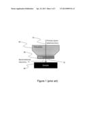
[0012] FIG. 1. is a diagram of a prior art electron microscope to detect backscattered electrons;
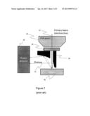
[0013] FIG. 2 is a diagram of a prior art electron microscope to detect backscattered electrons and photons
[0014] FIG. 3 is a diagram of an electron microscope to simultaneously detect backscattered electrons and photons, wherein the backscattered electron detector has a convex mirrored surface to reflect photons;
[0015] FIG. 4 is a diagram of an electron microscope to simultaneously detect backscattered electrons and cathodoluminesence, wherein the backscattered electron detector has a concave mirrored surface to reflect photons; and
[0016] FIG. 5 is a diagram of a further embodiment of an electron microscope to simultaneously detect backscattered electrons and cathodoluminesence wherein a small backscattered electron detector is mounted in a photon directing element.
DETAILED DESCRIPTION
[0017] FIG. 1 shows a standard electron microscope with a direct detection backscattered electron detector 30. The electron beam 10 is directed through the pole piece 20 and the detector 30 to the sample 40. Backscattered electrons 11 leave the surface of the sample 20 and are detected by the detector 30. The detector is a direct electron detector as opposed to a detector comprising a scintillator that converts electrons to photons.
[0018] FIG. 2 shows a prior art system for detecting cathodoluminescence photons 14 produced in the sample 40. A photon collection mirror 50 is placed between the backscattered electron detector 30 and the sample 40. Photons 12 produced by the sample 40 are directed by the mirror 50 to a photon detector 52. This configuration has the disadvantage that the mirror blocks a significant portion of the backscattered electrons from reaching the detector 30.
[0019] In an embodiment of the invention shown in FIG. 3, a semiconductor diode 60 for sensing backscattered electrons 11 (e.g. a silicon photodiode/avalanche diode) is shaped to direct photons 12 to an optical detector 62. A reflective coating applied to the diode 60 increases the reflectivity of the diode. Reflective coatings include aluminum and gold.
[0020] In an alternate embodiment, shown in FIG. 4, the diode 60 has a three dimensional concave surface 61, such as an ellipsoidal or paraboloidal surface. This type of surface collimates or focuses the photons 12 onto other optical instrumentation, which can also include a conduit of the light to an external photon detector, (e.g. PMT or photodiode, or it can be the actual detector itself).
[0021] In a further embodiment, shown in FIG. 5, a miniature backscattered electron detector 70 is mounted within a photon directing element 80. Mounting the detector 70 close to the reflective plane of the optical element 80 means that the detector functions at a short working distance, compensating for the reduction in size by maintaining a large solid angle for the detector 70. Use of a miniature backscattered electron detector minimizes solid angle loss of the photon collection optical element 80. If a concave optical element (e.g. paraboloidal or ellipsoidal) is used, angling of the backscattered electron detector to reflect photons towards the photon detector minimizes optical losses as a result of the sacrificed solid angle of the optical element.
[0022] In a further embodiment, the optical element 80 is made from conductive but highly reflective material e.g. diamond-turned aluminum.
[0023] In a further embodiment, the backscattered electron detector is a silicon diode supported on a carrier for physical support.
[0024] While the invention has been described in detail and with reference to specific examples thereof, it will be apparent to one skilled in the art that various changes and modifications can be made therein without departing from the spirit and scope thereof.
User Contributions:
Comment about this patent or add new information about this topic:
Images included with this patent application:
 |  |
| Similar patent applications: | |
| Date | Title |
|---|---|
| 2013-08-08 | Terahertz frequency domain spectrometer with discrete coarse and fine tuning |
| 2013-08-08 | Scintillation detection device with an encapsulated scintillator |
| 2013-08-01 | Deconvolution of time-gated cathodoluminescence images |
| 2011-11-03 | Stacked-electrode peptide-fragmentation device |
| 2013-07-18 | Optical encoder with signal offset correction system |
| New patent applications in this class: | |
| Date | Title |
|---|---|
| 2018-01-25 | Sparse sampling methods and probe systems for analytical instruments |
| 2018-01-25 | Electron beam inspection apparatus and electron beam inspection method |
| 2016-12-29 | Charged particle beam apparatus |
| 2016-09-01 | Near-field optical transmission electron emission microscope |
| 2016-07-14 | Inspection equipment |
| Top Inventors for class "Radiant energy" | |
| Rank | Inventor's name |
|---|---|
| 1 | Jason Lee Wildgoose |
| 2 | Osamu Wakabayashi |
| 3 | Toshio Kameshima |
| 4 | Tomoyuki Yagi |
| 5 | Katsuro Takenaka |