Patent application title: POWER-UP SIGNAL GENERATION CIRCUIT OF SEMICONDUCTOR APPARATUS
Inventors:
Yun Seok Hong (Icheon-Si, KR)
Assignees:
Hynix Semiconductor Inc.
IPC8 Class: AH03K300FI
USPC Class:
327544
Class name: Specific identifiable device, circuit, or system with specific source of supply or bias voltage power conservation or pulse type
Publication date: 2012-10-04
Patent application number: 20120249228
Abstract:
A power-up signal generation circuit of a semiconductor apparatus
includes a driver configured to generate a power-up signal in response to
a first voltage. The power-up signal generation circuit may also comprise
a power control unit configured to provide the first voltage or a second
voltage as a power supply voltage to the driver in response to the
power-up signal.Claims:
1. A power-up signal generation circuit of a semiconductor apparatus
comprising: a driver configured to generate a power-up signal in response
to a first voltage; and a power control unit configured to provide the
first voltage or a second voltage as a power supply voltage to the driver
in response to the power-up signal.
2. The power-up signal generation circuit according to claim 1, wherein the power control unit provides the first voltage as the power supply voltage to the driver after the power-up signal is asserted.
3. The power-up signal generation circuit according to claim 1, wherein the power control unit provides the second voltage as the power supply voltage to the driver before the power-up signal is asserted.
4. The power-up signal generation circuit according to claim 1, wherein the first voltage comprises one of internal voltages of the semiconductor apparatus.
5. The power-up signal generation circuit according to claim 1, wherein the second voltage is supplied from a node external to the semiconductor apparatus.
6. A power-up signal generation circuit comprising: a driver configured to generate a power-up signal in response to a power supply voltage and an input voltage; and a power control unit configured to change the power supply voltage to a voltage having the same level as the input voltage after the power-up signal is asserted.
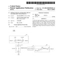
7. The power-up signal generation circuit according to claim 6, wherein the power control unit provides an external voltage as the power supply voltage to the driver before the power-up signal is asserted, wherein the external voltage is supplied from a node external to the semiconductor apparatus.
8. The power-up signal generation circuit according to claim 6, wherein the input voltage comprises one of internal voltages of the semiconductor apparatus.
9. A power-up signal generation circuit comprising: a driver configured to generate a preliminary power-up signal in response to a first voltage; a signal combination unit configured to combine the preliminary power-up signal and a test mode signal and generate a power-up signal; and a power control unit configured to provide the first voltage or a second voltage as a power supply voltage to the driver in response to the power-up signal.
10. The power-up signal generation circuit according to claim 9, further comprising a level shifter configured to shift the preliminary power-up signal to the level of the second voltage and provide the shifted signal to the signal combination unit.
11. The power-up signal generation circuit according to claim 9, wherein the power control unit provides the first voltage as the is power supply voltage to the driver after the power-up signal is asserted.
12. The power-up signal generation circuit according to claim 9, wherein the power control unit provides the second voltage as the power supply voltage to the driver before the power-up signal is asserted.
13. The power-up signal generation circuit according to claim 9, wherein the first voltage comprises one of internal voltages of the semiconductor apparatus.
14. The power-up signal generation circuit according to claim 9, wherein the second voltage comprises an external voltage, wherein the external voltage is supplied from a node external to the semiconductor apparatus.
15. The power-up signal generation circuit according to claim 9, comprising circuitry to force the power-up signal to remain asserted during a test mode.
16. A method of generating a power-up signal in a semiconductor apparatus, comprising: generating a first power-up signal in response to a first voltage, wherein a power-up signal is generated from the first power-up signal; and providing the first voltage or a second voltage in response to the power-up signal as a power supply voltage to generate the first power-up signal.
17. The method of generating a power-up signal in a semiconductor apparatus according to claim 16, wherein the first voltage is provided as the power supply voltage after the power-up signal is asserted.
18. The method of generating a power-up signal in a semiconductor apparatus according to claim 16, wherein the second voltage is provided as the power supply voltage before the power-up signal is asserted.
19. The method of generating a power-up signal in a semiconductor apparatus according to claim 16, wherein the first voltage comprises one of internal voltages of the semiconductor to apparatus.
20. The method of generating a power-up signal in a semiconductor apparatus according to claim 16, wherein the second voltage comprises an external voltage, wherein the external voltage is is supplied from a node external to the semiconductor apparatus.
Description:
CROSS-REFERENCES TO RELATED APPLICATION
[0001] The present application claims priority under 35 U.S.C. §119(a) to Korean application number 10-2011-0027580 filed on Mar. 28, 2011 in the Korean Intellectual Property Office, which is incorporated by reference in its entirety.
BACKGROUND
[0002] 1. Technical Field
[0003] The present invention relates to a semiconductor apparatus, and more particularly, to a power-up signal generation circuit.
[0004] 2. Related Art
[0005] A semiconductor apparatus generates a variety of internal voltages VPERI and VCORE using an external voltage VDD.
[0006] The semiconductor apparatus detects whether the above-described voltages approach a predetermined level or not, and generates power-up signals for the respective internal voltages. Accordingly, the semiconductor apparatus performs a reset process and then performs various operations after various circuitry have been reset to a known state.
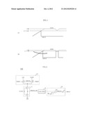
[0007] For example, referring to FIG. 1A, a power-up signal PWRUP may be generated when an internal voltage VPERI approaches a predetermined level, that is, a trigger level (for example, 0.7-0.8V).
[0008] At this time, the trigger level corresponds to the level of the internal voltage, at which the power-up signal PWRUP changes.
[0009] A minimum level of the internal voltage VPERI is required for performing stable operation in the semiconductor apparatus. The minimum level may be, for example, a target level of 1.35V.
[0010] In this case, since the trigger level is lower than the target level of the internal voltage VPERI, it is highly likely that a reset error may occur in the semiconductor apparatus.
[0011] Therefore, in order to prevent such an error, the trigger level of the internal voltage VPERI may be increased to 1.1-1.2V, as shown in FIG. 1B.
[0012] In this method, however, when the level of the internal voltage VPERI temporarily decreases during normal operation, the is power-up signal PWRUP may be regenerated to reset the semiconductor apparatus.
SUMMARY
[0013] A power-up signal generation circuit of a semiconductor apparatus, which is capable of increasing the trigger level of a power-up signal and preventing the regeneration of a power-up signal during a normal operation, is described.
[0014] In one embodiment of the present invention, a power-up signal generation circuit of a semiconductor apparatus includes a driver configured to generate a power-up signal in response to a first voltage, where a power-up signal is generated from the first power-up signal. The power-up signal generation circuit may also comprise a power control unit configured to provide the first voltage or a second voltage as a power supply voltage to the driver in response to the power-up signal.
[0015] In another embodiment of the present invention, a power-up signal generation circuit includes a driver configured to generate a power-up signal in response to a power supply voltage and an input voltage, and a power control unit configured to change the power supply voltage to a voltage having the same level as the input voltage after the power-up signal is activated.
[0016] In another embodiment of the present invention, a power-up signal generation circuit includes a driver configured to generate a is preliminary power-up signal in response to a first voltage, a signal combination unit configured to combine the preliminary power-up signal and a test mode signal and generate a power-up signal, and a power control unit configured to provide the first voltage or a second voltage as a power supply voltage to the driver in response to the power-up signal.
[0017] In another embodiment of the present invention, a method of generating a power-up signal in a semiconductor apparatus, may comprise generating a first power-up signal in response to a first voltage, wherein a power-up signal is generated from the first power-up signal, and provide the first voltage or a second voltage in response to the power-up signal as a power supply voltage to generate the first power-up signal.
BRIEF DESCRIPTION OF THE DRAWINGS
[0018] Features, aspects, and embodiments are described in conjunction with the attached drawings:
[0019] FIGS. 1A and 1B are waveform diagrams showing the waveform of a power-up signal in a convention semiconductor apparatus; and
[0020] FIG. 2 is a circuit diagram of a power-up signal generation circuit according to one embodiment of the invention.
DETAILED DESCRIPTION
[0021] A power-up signal generation circuit of a semiconductor apparatus according to various embodiments of the present invention will be described below with reference to the accompanying drawings.
[0022] A semiconductor apparatus may generate various internal voltages such as, for example, VPERI and VCORE using an external voltage VDD.
[0023] The semiconductor apparatus detects whether the above-described voltages approach a trigger level or not, and completes power-up operations for the respective voltages, that is, generates power-up signals. Accordingly, the semiconductor apparatus performs a reset process and then performs various operations related to the function of the semiconductor apparatus.
[0024] The trigger level corresponds to the level of an internal voltage at which a power-up signal PWRUP is generated.
[0025] That is, the trigger level is where the power-up signal PWRUP changes from a high level to a low level.
[0026] A power-up signal generation circuit according to one embodiment is configured to generate power-up signals PWRUP for various voltage levels requiring a power-up operation, which include internal voltages VPERI and VCORE.
[0027] In this embodiment, a case in which a power-up signal PWRUP for the internal voltage VCORE is generated will be taken as an example.
[0028] Referring to FIG. 2, the power-up signal generation circuit 100 of the semiconductor apparatus according to an embodiment of the invention includes a driver 110, a power control unit 120, a level shifter 140, and a signal combination unit 130.
[0029] The driver 110 is configured to drive an input voltage, that is, a first voltage, and generate a preliminary power-up signal PWRUP_PRE.
[0030] The driver 110 includes transistors P1 and N1 coupled in an inverter structure.
[0031] The power control unit 120 is configured to provide a second voltage as a power supply voltage of the driver 110 before a power-up operation is completed, and provide the first voltage as a power supply voltage of the driver 110 after the power-up operation is completed.
[0032] The power control unit 120 is configured to provide the first or second voltage as a power supply voltage of the driver 110, in response to power-up signals PWRUP and PWRUPB.
[0033] The power-up signal PWRUP is a signal obtained by inverting the power-up signal PWRUPB.
[0034] The first voltage may include an inverter voltage VCORE, and the second voltage may include an external voltage VDD.
[0035] The power control unit 120 includes pass gates T1 and T12.
[0036] The pass gate T1 has NMOS and PMOS gates configured to receive the power-up signals PWRUP and PWRUPB, respectively, a source configured to receive an external voltage VDD, and a drain is coupled to a source of a transistor P1 of the driver 110.
[0037] The pass gate T2 has NMOS and PMOS gates configured to receive the power-up signals PWRUPB and PWRUP, respectively, a source configured to receive an internal voltage VCORE, and a drain coupled to the source of the transistor P1 of the driver 110.
[0038] The level shifter 140 is configured to shift the preliminary power-up signal PWRUP_PRE having a level of the internal voltage VCORE to the level of the external voltage VDD.
[0039] The signal combination unit 130 is configured to combine an output of the level shifter 140 and a test mode signal TM and output the power-up signals PWRUP and PWRUPB.
[0040] The signal combination unit 130 includes a NAND gate ND1 and inverters IV1 and IV2.
[0041] The test mode signal TM may be used for tests that may not require generating the PWRUP signal from the internal voltage VCORE, for example.
[0042] For example, when the test mode signal TM is asserted to a high level to perform a specific test mode, the NAND gate ND1 outputs a high-level signal regardless of the level of the internal voltage VCORE. Accordingly, the power-up signal PWRUP may be at a low level as long as the test mode signal TM is asserted to a high level.
[0043] Therefore, since the change of the power-up signal PWRUP is prevented, the specific test mode in which the internal voltage VCORE is not used may be performed.
[0044] The power-up operation of the power-up signal generation circuit according to an embodiment of the invention will be described as follows.
[0045] During the initial operation, the internal voltage VCORE is at a low level, but the external voltage VDD is at a normal level. Therefore, the driver 110 outputs the preliminary power-up signal PWRUP_PRE at a high level.
[0046] The preliminary power-up signal PWRUP_PRE is passed through the level shifter 140 and output at a high level of the external voltage VDD. Accordingly, the signal combination unit 130 outputs a high-level power-up signal PWRUP.
[0047] That is, during the initial operation when the internal voltage VCORE is ramping up, the power-up signal PWRUP has a high level.
[0048] Since the power-up signal PWRUP is at a high-level, the power control unit 120 provides the external voltage VDD as a power supply voltage to the driver 110.
[0049] When the internal voltage VCORE rises to approach a predetermined trigger level, the power-up signal PWRUP changes to a low level. That is, as the power-up signal PWRUP is generated, an initial normal power-up operation is performed.
[0050] Since the power-up signal PWRUP changed to a low level, the power control unit 120 provides the internal voltage VCORE as a power supply voltage to the driver 110.
[0051] That is, the source and gate levels of the driver 110 are is equalized.
[0052] Therefore, although the internal voltage VCORE is varied, the driver 110 maintains the preliminary power-up signal PWRUP_PRE to a low level.
[0053] Accordingly, although the internal voltage VCORE may fluctuate after the power-up signal PWRUP was generated at the initial stage, the power-up signal PWRUP is not regenerated.
[0054] According to various embodiments of the present invention, the reset operation of the semiconductor apparatus may be stably performed, and the regeneration of the power-up signal may be substantially prevented.
[0055] While certain embodiments have been described above, it will be understood to those skilled in the art that the embodiments described are by way of example only. Accordingly, the power-up signal generation circuit described should not be limited based on the described embodiments. Rather, the power-up signal generation circuit described should only be limited in light of the claims that follow when taken in conjunction with the above description and accompanying drawings.
User Contributions:
Comment about this patent or add new information about this topic:
Images included with this patent application:
 |  |
| Similar patent applications: | |
| Date | Title |
|---|---|
| 2013-05-23 | Power-up signal generation circuit |
| 2013-06-06 | Power-up signal generation circuit |
| 2012-10-11 | Multi-layered semiconductor apparatus |
| 2010-06-10 | Trigger signal detection apparatus |
| 2012-09-13 | Pll circuit and optical disc apparatus |
| New patent applications in this class: | |
| Date | Title |
|---|---|
| 2016-04-21 | Control chip and system using the same for power saving |
| 2016-02-04 | Semiconductor integrated circuit device |
| 2015-04-23 | Closed-loop adaptive voltage scaling for integrated circuits |
| 2014-09-04 | Minimizing power consumption in asynchronous dataflow architectures |
| 2014-06-19 | Dynamic clock and power gating with decentralized wake-ups |
| New patent applications from these inventors: | |
| Date | Title |
|---|---|
| 2014-12-18 | Driving device |
| 2014-05-29 | Initialization circuit |
| 2013-07-04 | Internal voltage generation circuit |
| 2011-10-06 | Self refresh circuit |
| 2011-02-03 | Test device for testing transistor characteristics in semiconductor integrated circuit |
| Top Inventors for class "Miscellaneous active electrical nonlinear devices, circuits, and systems" | |
| Rank | Inventor's name |
|---|---|
| 1 | Yantao Ma |
| 2 | Feng Lin |
| 3 | Ming-Chieh Huang |
| 4 | Yong-Ju Kim |
| 5 | Chan-Hong Chern |