Patent application title: Primary-side controlled power converter with an RC network and Method thereof
Inventors:
Ta-Yung Yang (Mulpitas, CA, US)
Assignees:
SYSTEM GENERAL CORPORATION
IPC8 Class: AH02M3335FI
USPC Class:
363 2112
Class name: Single-ended, separately-driven type with automatic control of the magnitude of output voltage or current for flyback-type converter
Publication date: 2012-07-05
Patent application number: 20120170326
Abstract:
This invention provides a primary-side controlled power converter
comprising: an RC network coupled to an auxiliary winding of a
transformer of the primary-side controlled power converter to detect a
reflected voltage of the transformer for generating a reflected signal,
and a controller coupled to the RC network to receive the reflected
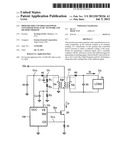
signal for generating a switching signal; wherein the RC network develops
a zero to provide a high-frequency path for shortening a rising time and
a settling time of the reflected signal.Claims:
1. A primary-side controlled power converter, comprising: an RC network
coupled to an auxiliary winding of a transformer of the primary-side
controlled power converter to detect a reflected voltage of the
transformer to generate a reflected signal; and a controller coupled to
the RC network to receive the reflected signal and generate a switching
signal; wherein the RC network develops a zero to provide a
high-frequency path to shorten a rising time and a settling time of the
reflected signal.
2. The power converter as claimed in claim 1, wherein the RC network comprises: a first resistor coupled to the auxiliary winding to detect the reflected voltage of the transformer; a third resistor serially connected with the first resistor; a second resistor connected from the third resistor to ground; a high-pass capacitor parallel connected to the first resistor; a low-pass capacitor parallel connected to the second resistor; wherein the controller is coupled to a join of the second resistor and the low-pass capacitor.
3. The power converter as claimed in claim 2, wherein the first resistor has a first terminal and a second terminal, the first terminal of the first resistor being coupled to the auxiliary winding of the transformer; the third resistor has a first terminal and a second terminal, the first terminal of the third resistor being connected to the second terminal of the first resistor.
4. The power converter as claimed in claim 1, wherein the controller generates the switching signal according to the reflected voltage for regulating an output voltage of the power converter.
5. The power converter as claimed in claim 1, wherein the controller generates the switching signal according to the reflected voltage for regulating an output current of the power converter.
6. A primary-side controlled power converter with a network, the network comprising: a resistor coupled to an auxiliary winding of a transformer of the primary-side controlled power converter to detect a reflected voltage of the transformer; a high-pass capacitor connected to the resistor in parallel; a controller coupled to the resistor to receive the reflected voltage; wherein the resistor and the high-pass capacitor develop a zero of the network, and the controller generates a switching signal according to the reflected voltage.
7. The power converter as claimed in claim 6, wherein a reflected signal is generated at a join of the network and the controller, and the resistor and the high-pass capacitor provide a high-frequency path of the network to shorten a rising time and a settling time of the reflected signal.
8. The power converter as claimed in claim 6, wherein the controller generates the switching signal according to the reflected voltage for regulating an output voltage of the power converter.
9. The power converter as claimed in claim 6, wherein the controller generates the switching signal according to the reflected voltage for regulating an output current of the power converter.
10. A method for detecting a reflected voltage of a transformer of a primary-side controlled power converter, comprising: coupling an RC network between an auxiliary winding of the transformer of the primary-side controlled power converter and a controller, wherein the RC network develops a zero to provide a high-frequency path; receiving a reflected signal generated at a join of the RC network and the controller; generating a switching signal according to the reflected signal through the controller.
11. The method as claimed in claim 10, the RC network comprises: a first resistor coupled to the auxiliary winding; a third resistor serially connected with the first resistor; a second resistor connected from the third resistor to ground; a high-pass capacitor parallel connected to the first resistor; a low-pass capacitor parallel connected to the second resistor; wherein the controller is coupled to a join of the second resistor and low-pass capacitor.
Description:
BACKGROUND OF THE INVENTION
[0001] 1. Field of the invention
[0002] The present invention relates to a power converter, and more particularly, to a primary-side controlled power converter with an RC network.
[0003] 2. Description of related art
[0004] Pulse Width Modulation (PWM) technique is widely used in power converters to regulate output voltage to an appropriate level. In order to reduce the number of elements in the power converter and dispense with a secondary-side feedback circuit, a primary-side control technique has been developed. To achieve the primary-side control, a reflected voltage on an auxiliary winding of a transformer can be sensed for voltage feedback control. However, the reflected voltage sensed on the auxiliary winding is not as accurate as a signal sensed directly on the secondary-side of the power converter. Moreover, high-frequency noise and ringing exist in the reflected voltage.
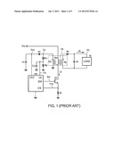
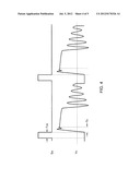
[0005] FIG. 1 shows a circuit diagram of a conventional primary-side controlled power converter. The primary-side controlled power converter comprises a transformer 10 including a primary winding NP, a secondary winding NS, and an auxiliary winding NA. An anode of a rectifier 40 is coupled to the auxiliary winding NA. One terminal of a storage capacitor 45 is connected to a cathode of the rectifier 40. The other terminal of the storage capacitor 45 is connected to ground. A switching controller 100 is coupled to sample a reflected voltage VA of the auxiliary winding NA of the transformer 10 through a low-pass filter. The low-pass filter includes resistors RA, RB and a capacitor C2. The resistor RA is connected to the auxiliary winding NA to receive the reflected voltage VA. The capacitor C2 is connected to a join of the resistors RA and RB. The capacitor C2 is used for filtering noises and providing a path with low impedance for EMI. A reflected signal VS is generated at a join of the capacitor C2, the resistor RA, and the resistor RB and received by the switching controller 100. The switching controller 100 generates the switching signal SW based on the reflected signal VS to switch the transformer 10 by switching a power transistor 20. When the power transistor 20 is turned off and the switching signal SW is during an off-time period, the reflected voltage VA is generated accordingly. The waveforms of the switching signal SW and the reflected signal VS are shown in FIG. 2. The transfer function of the reflected signal VS and the reflected voltage VA can be expressed as follows:
V S V A = Z 2 R A + Z 2 = R B 1 + SR B C A R A + R B 1 + SR B C A = R B R A + R B + SR A R B C A = R B R A + R B × 1 1 + S R A × R B R A + R B C A ( 1 ) V S V A = R B R A + R B × 1 1 + j ( f f A ) ( 2 ) f A = 1 2 π × ( R A × R B R A + R B ) × C A ( 3 ) ##EQU00001##
[0006] where the frequency fA is a pole of the transfer function of the reflected signal VS and the reflected voltage VA. When the switching signal SW changes from high level to low level and the power transistor 20 is turned off, the reflected signal VS starts to rise. A settling time TD of the reflected signal VS is determined by the frequency fA.
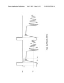
[0007] FIG. 2 illustrates waveforms of the switching signal SW and the reflected signal VS in the conventional primary-side controlled power converter of FIG I. After the reflected signal VS has been filtered by the low-pass filter, the rising time and the settling time TD thereof are prolonged. The low-pass filter further limits the maximum frequency of the switching signal SW. Therefore, to reduce the settling time TD and to allow increase of the maximum frequency of the switching signal SW are desired.
SUMMARY OF THE INVENTION
[0008] An object of the present invention is to reduce the settling time TD and increase the maximum frequency of the switching signal SW.
[0009] To achieve the aforementioned object, the present invention provides a primary-side controlled power converter comprising: an RC network coupled to an auxiliary winding of a transformer of the primary-side controlled power converter to detect a reflected voltage of the transformer so as to generate a reflected signal; and a controller coupled to the RC network to receive the reflected signal so as to generate a switching signal; wherein the RC network develops a zero to provide a high-frequency path so as to shorten a rising time and a settling time of the reflected signal.
[0010] The foregoing RC network comprises: a first resistor having a first terminal and a second terminal, the first terminal of the first resistor being coupled to the auxiliary winding of the transformer to detect the reflected voltage of the transformer; a third resistor having a first terminal and a second terminal, the first terminal of the third resistor being connected to the second terminal of the first resistor; a second resistor connected to the second terminal of the third resistor and ground; a first capacitor connected to the first resistor in parallel; and a second capacitor connected to the second resistor in parallel.
[0011] To achieve the foregoing object, the present invention further provides a method for detecting a reflected voltage of a transformer of a primary-side controlled power converter, comprising: coupling an RC network to an auxiliary winding of the transformer of the primary-side controlled power converter, wherein the RC network develops a zero to provide a high-frequency path; receiving a reflected signal generated by the RC network; and generating a switching signal based on the reflected signal.
BRIEF DESCRIPTION OF THE DRAWINGS
[0012] FIG. 1 illustrates a circuit diagram of a conventional primary-side controlled power converter.
[0013] FIG. 2 illustrates waveforms of the switching signal and the reflected signal in the conventional primary-side controlled power converter of FIG. 1.
[0014] FIG. 3 illustrates a circuit diagram of a primary-side controlled power converter according to one embodiment of the present invention.
[0015] FIG. 4 illustrates waveforms of the switching signal and the reflected signal according to one embodiment of the present invention.
[0016] FIG. 5 illustrates a circuit diagram of a controller according to one embodiment of the present invention.
DETAILED DESCRIPTION OF THE INVENTION
[0017] FIG. 3 is a circuit diagram of a primary-side controlled power converter according to one embodiment of the present invention. The primary-side controlled power converter comprises a transformer 10 including a primary winding NP, a secondary winding NS and an auxiliary winding NA. One terminal of the primary winding NP receives an input voltage VIN. The other terminal of the primary winding NP is coupled to a drain terminal of a power transistor 20. An anode of an output rectifier 60 is coupled to one terminal of the secondary winding NS. One terminal of an output capacitor 65 is connected to a cathode of the output rectifier 60. The other terminal of the output capacitor 65 is connected to the other terminal of the secondary winding NS. An output current IO flows through an output load 70 connected to the output capacitor 65 in parallel. An output voltage VO is generated at one terminal of the output capacitor 65. An anode of a rectifier 40 is coupled to the auxiliary winding NA. One terminal of a storage capacitor 45 is connected to a cathode of the rectifier 40. The other terminal of the storage capacitor 45 is connected to ground. A supply voltage VCC is generated at a join of the storage capacitor 45 and the cathode of the rectifier 40.
[0018] The primary-side controlled power converter comprises an RC network coupled to the auxiliary winding NA of the transformer 10 to detect a reflected voltage VA of the transformer so as to generate a reflected signal VS and a controller 100 coupled to the RC network to receive the reflected signal VS so as to generate a switching signal SW. An RC network includes a first resistor R1, a second resistor R2, a third resistor R3, a high-pass capacitor C1, and a low-pass capacitor C2. A first terminal of the first resistor R1 is coupled to the auxiliary winding NA of the transformer 10 of the primary-side controlled power converter to detect the reflected voltage VA of the transformer 10. A first terminal of the third resistor R3 is connected to a second terminal of the first resistor R1. A first terminal of the second resistor R2 is connected to a second terminal of the third resistor R3, and the second terminal of the second resistor R2 is connected to ground.
[0019] A first terminal of the high-pass capacitor C1 is coupled to the auxiliary winding NA of the transformer 10 and the first terminal of the first resistor R1. A second terminal of the high-pass capacitor C1 is connected to the second terminal of the first resistor R1. In other words, the high-pass capacitor C1 is connected to the first resistor R1 in parallel. A first terminal of the low-pass capacitor C2 is coupled to the second terminal of the third resistor R3, and the second terminal of the second resistor R2. A second terminal of the low-pass capacitor C2 is connected to ground. In other words, the low-pass capacitor C2 is connected to the second resistor R2 in parallel. The second terminal of the low-pass capacitor C2, the second terminal of the third resistor R3, and the first terminal of the second resistor R2 are further connected to a terminal VS of the controller 100. The reflected signal VS is generated at the terminal VS of the controller 100. The switching signal SW is generated at an output terminal SW of the controller 100 and used to control the power transistor 20. A primary-side switching current IP is generated when the power transistor 20 is turned on and the switching signal SW is during an on-time period. A current-sense signal VCS is generated at a join of a current-sense terminal CS of the controller 100, one terminal of a current-sense resistor 30, and a source of the power transistor 20 in response to the primary-side switching current IP. The other terminal of the current-sense resistor 30 is connected to ground. The supply voltage VCC is generated at a supply terminal VCC of the controller 100.
[0020] The Laplace transform of the transfer function of the reflected signal VS and the reflected voltage VA can be expressed as follows:
V S V A = R 2 1 + SR 2 C 2 R 3 + R 1 1 + SR 1 C 1 + R 2 1 + SR 2 C 2 = R 2 ( 1 + SR 1 C 1 ) R 3 ( 1 + SR 1 C 1 ) ( 1 + SR 2 C 2 ) + R 1 ( 1 + SR 2 C 2 ) R 2 ( 1 + SR 1 C 1 ) = R 2 R 3 + R 2 + R 1 × ( 1 + SR 1 C 1 ) [ ( S 2 R 1 R 2 R 3 R 3 + R 2 + R 1 C 1 C 2 ) + S ( R 3 R 1 C 1 + R 3 R 2 C 2 + R 1 R 2 C 2 + R 2 R 1 C 1 R 3 + R 2 + R 1 ) + R 3 + R 2 + R 1 R 3 + R 2 + R 1 ] = R 2 R 3 + R 2 + R 1 × ( 1 + SR 1 C 1 ) S 2 ( R 3 R 2 R 1 R 3 + R 2 + R 1 C 2 C 1 ) + S ( R 3 R 1 C 1 + R 3 R 2 C 2 + R 2 R 1 C 2 + R 2 R 1 C 1 R 3 + R 2 + R 1 ) + 1 ( 4 ) V S V A = R 2 R 3 + R 2 + R 1 × 1 + j ( f f 1 ) [ 1 + j ( f f X ) ] × [ 1 + j ( f f Y ) ] ( 5 ) f 1 = 1 2 π × R 1 × C 1 ( 6 ) ##EQU00002##
[0021] The transfer function of the reflected signal VS and the reflected voltage VA can be simplified as the formula (5), where a first frequency f1 is a zero; a second frequency fX and a third frequency fY are poles. The zero is determined by the first resistor R1 and the high-pass capacitor C1, which provides a high-frequency path so as to shorten the rising time and the settling time TD of the reflected voltage VA. The waveforms of the switching signal SW and the reflected signal VS are shown in FIG. 4. Compared to FIG. 2, the rising time and the settling time TD of the reflected signal VS have been shortened and the rising edge of the reflected signal VS has a sharper gradient.
[0022] FIG. 5 illustrates a preferred embodiment of the controller 100 for the primary-side controlled power converter. The detailed description of the primary-side controlled power converter can be found in the following references: U.S. Pat. No. 6,977,824, entitled "Control circuit for controlling output current at the primary side of a power converter"; U.S. Pat. No. 7,016,204, entitled "Close-loop PWM controller for primary-side controlled power converters"; U.S. Pat. No. 7,349,229, entitled "Causal sampling circuit for measuring reflected voltage and demagnetizing e of transformer"; U.S. Pat. No. 7,486,528, entitled "Linear-predict sampling for measuring demagnetized voltage of transformer".
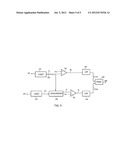
[0023] The controller 100 comprises a voltage-detection circuit 150, a current-detection circuit 200, an integrator 250, amplifiers 350 and 370, low-pass filters 400 and 450, and a PWM circuit 500. The voltage-detection circuit 150 receives the reflected signal VS at the terminal VS to generate a voltage-feedback signal VV and a discharge-time signal SDS. A first reference signal VRV is applied to a positive input of the amplifier 350 and the voltage-feedback signal VV is applied to a negative input of the amplifier 350. The amplifier 350 can be implemented as an error amplifier according to one embodiment of the present invention. By comparing the voltage-feedback signal VV with the reference signal VRV, the amplifier 350 amplifies the voltage-feedback signal VV and outputs an amplified signal EV for providing a voltage loop of the controller 100. The amplified signal EV is received by the low-pass filter 400 to generate a voltage-loop signal VCOMV for the frequency compensation of the voltage loop.
[0024] The current-detection circuit 200 is coupled to the current-sense resistor 30 and the power transistor 20 (shown in FIG. 3) to receive the current-sense signal VCS so as to generate a current-waveform signal VW. The current-sense signal VCS is generated at the current-sense terminal CS of the controller 100. The integrator 250 is coupled to the current-detection circuit 200 and the voltage-detection circuit 150 so as to generate a current-feedback signal VI based on the current-waveform signal VW and the discharge-time signal SDS. The current-waveform signal VW is generated by measuring the primary-side switching current IP. The current-feedback signal VI is generated by integrating the current-waveform signal VW with the discharge-time signal SDS. A second reference current signal VRI is applied to the positive terminal of the amplifier 370. The current-feedback signal VI is further applied to a negative input of the amplifier 370. By comparing the current-feedback signal VI and the second reference current signal VRI, the amplifier 370 amplifies the current-feedback signal VI and generates an amplified signal EI for providing a current loop of the controller 100. The amplified signal EI is received by the low-pass filter 450 to generate a current-loop signal VCOMI for the frequency compensation of the current loop. The PWM circuit 500 generates the switching signal SW and controls a pulse width of the switching signal SW responding to the voltage-loop signal VCOMV and the current-loop signal VCOMI. Hence, the controller 100 is coupled to the RC network to receive the reflected signal VS for generating the switching signal SW.
[0025] Although the present invention and the advantages thereof have been described in detail, it should be understood that various changes, substitutions, and alternations can be made therein without departing from the spirit and scope of the invention as defined by the appended claims. That is, the discussion included in this invention is intended to serve as a basic description. It should be understood that the specific discussion may not explicitly describe all embodiments possible; many alternatives are implicit. The generic nature of the invention may not fully explained and may not explicitly show that how each feature or element can actually be representative of a broader function or of a great variety of alternative or equivalent elements. Again, these are implicitly included in this disclosure. Neither the description nor the terminology is intended to limit the scope of the claims.
User Contributions:
Comment about this patent or add new information about this topic:
Images included with this patent application:
 |  |
 |  |
 |  |
| Similar patent applications: | |
| Date | Title |
|---|---|
| 2013-05-09 | Dynamic power factor correction and dynamic control for converter in power supply |
| 2010-07-01 | Current controlled power converter |
| 2012-05-03 | Current controlled power converter |
| 2013-04-18 | Composite ac-to-dc power converter using midpoint method |
| 2013-04-25 | Power converter systems and methods of operating a power converter system |
| New patent applications in this class: | |
| Date | Title |
|---|---|
| 2022-05-05 | Multi-mode control method for active clamp flyback converter |
| 2017-08-17 | Phase-cut pre-regulator and power supply comprising the same |
| 2016-12-29 | Power conversion device |
| 2016-12-29 | Switching power converter with adaptive power factor correction |
| 2016-12-29 | Integrated circuit and switching power-supply device |
| New patent applications from these inventors: | |
| Date | Title |
|---|---|
| 2012-12-06 | High-side signal sensing circuit |
| 2012-09-13 | Switching controller with valley-lock switching and limited maximum frequency for quasi-resonant power converters |
| 2012-08-23 | Adaptive filter circuit for sampling a reflected voltage of transformer in a power converter and method thereof |
| Top Inventors for class "Electric power conversion systems" | |
| Rank | Inventor's name |
|---|---|
| 1 | Ta-Yung Yang |
| 2 | Lieyi Fang |
| 3 | Alex B. Djenguerian |
| 4 | Martin Fornage |
| 5 | Balu Balakrishnan |