Patent application title: ELECTRONIC DEVICE
Inventors:
Keisuke Kuroda (Osaka, JP)
Keisuke Kuroda (Osaka, JP)
Assignees:
PANASONIC CORPORATION
IPC8 Class: AH03M106FI
USPC Class:
341118
Class name: Coded data generation or conversion converter compensation
Publication date: 2011-08-25
Patent application number: 20110205092
Abstract:
An electronic device includes a frequency variable circuit, a filter, and
an output voltage decision circuit. The frequency variable circuit
changes the sampling frequency of an analog-digital converter. The filter
limits the pass band of the output signal of the analog-digital
converter. The output voltage decision circuit determines the noise level
of the output signal of the analog-digital converter after the output
signal passes through the filter. The electronic device performs
self-diagnosis as follows. The frequency variable circuit changes the
sampling frequency of the analog-digital converter to a frequency outside
of the pass band of the filter so as to change the quantization noise
level of the analog-digital converter. Then, the output voltage decision
circuit determines whether the integral of the quantization noise level
is within a predetermined range.Claims:
1. An electronic device comprising: a detection device; a pick up circuit
for detecting, as a signal, physical information detected by the
detection device; an analog-digital (AD) converter for AD converting the
signal detected by the pick up circuit; a frequency variable circuit for
changing a sampling frequency of the analog-digital converter; a filter
for limiting a pass band of an output signal of the analog-digital
converter; and an output voltage decision circuit for calculating an
integral of a noise level of the output signal of the analog-digital
converter after the output signal passes through the filter, wherein the
electronic device performs self-diagnosis by making the frequency
variable circuit change the sampling frequency of the analog-digital
converter to a frequency outside of the pass band of the filter so as to
change a quantization noise level of the analog-digital converter, and
then by making the output voltage decision circuit determine whether the
integral of the quantization noise level is within a predetermined range
or not.
2. The electronic device of claim 1, wherein the physical information detected by the detection device is an angular velocity applied to the detection device.
3. The electronic device of claim 1, wherein the filter is a low-pass filter.
4. The electronic device of claim 3, wherein the filter comprises: a first amplifier for receiving the output signal of the analog-digital converter; a delay device for receiving the output signal of the analog-digital converter; a second amplifier for receiving an output signal of the delay device, and an adder circuit for adding output signals of the first and second amplifiers and outputting an addition result.
Description:
TECHNICAL FIELD
[0001] The present invention relates to electronic devices, such as automobiles, aircrafts, ships, robots, digital cameras, car navigation systems, and sensors.
BACKGROUND ART
[0002] FIG. 6 is an electrical diagram of a conventional electronic device. The electronic device includes detection device 1, pick up circuit 2, analog-digital (AD) converter 3, frequency supply circuit 4, output voltage decision circuit 7, and diagnosis signal supply circuit 8. Pick up circuit 2 detects, as a signal, physical information detected by detection device 1. Analog-digital converter 3 AD converts the signal detected by pick up circuit 2. Frequency supply circuit 4 determines the sampling frequency of analog-digital converter 3. Output voltage decision circuit 7 determines the magnitude of the output voltage of the output signal of analog-digital converter 3. Diagnosis signal supply circuit 8 supplies an analog signal for failure diagnosis to analog-digital converter 3. The self-diagnosis of the electronic device is completed when output voltage decision circuit 7 determines whether the output signal of analog-digital converter 3 which has received the analog signal is within a predetermined range. An example of a conventional technique related to the present invention is shown in Patent Literature 1.
Citation List
[0003] Patent Literature [0004] Patent Literature 1: Japanese Patent Unexamined Publication No. 2008-157719
SUMMARY OF THE INVENTION
[0005] In such a conventional electronic device, it is difficult to reduce the circuit size.
[0006] More specifically, in order to perform self-diagnosis, the conventional electronic device needs to have diagnosis signal supply circuit 8 for supplying an analog signal for failure diagnosis. This makes it difficult to reduce the circuit size of the electronic device.
[0007] The present invention is directed to provide an electronic device which has a compact circuit with a self-diagnosis function. The electronic device of the present invention includes a frequency variable circuit, a filter, and an output voltage decision circuit. The frequency variable circuit changes the sampling frequency of an analog-digital converter. The filter limits the pass band of the output signal of the analog-digital converter. The output voltage decision circuit calculates the integral of the noise level of the output signal of the analog-digital converter after the output signal passes through the filter. The electronic device performs self-diagnosis as follows. The frequency variable circuit changes the sampling frequency of the analog-digital converter to a frequency outside of the pass band of the filter so as to change the quantization noise level of the analog-digital converter. Then, the output voltage decision circuit determines whether the integral of the quantization noise level is within a predetermined range.
[0008] With this structure, the electronic device has a circuit with a self-diagnosis function without providing a diagnosis signal supply circuit for supplying an analog signal for failure diagnosis. As a result, the circuit of the electronic device can be compact.
BRIEF DESCRIPTION OF THE DRAWINGS
[0009] FIG. 1 is an electrical diagram of an electronic device according to a first exemplary embodiment of the present invention. FIG. 2 is an electrical diagram of another example of the electronic device according to the first exemplary embodiment of the present invention.
[0010] FIG. 3 is an electrical diagram of a filter in the electronic device according to the first exemplary embodiment of the present invention. FIG. 4 shows the relation between sampling frequency and quantization noise of an analog-digital converter in the electronic device according to the first exemplary embodiment of the present invention.
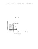
[0011] FIG. 5 shows the relation between a sampling frequency and a quantization noise after the output signal of the analog-digital converter passes through the filter in the electronic device according to the first exemplary embodiment of the present invention. FIG. 6 is an electrical diagram of a conventional electronic device.
DETAILED DESCRIPTION OF PREFERRED EMBODIMENT
First Exemplary Embodiment
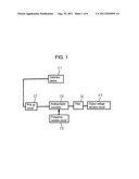
[0012] An electronic device according to a first exemplary embodiment of the present invention will be described as follows with reference to drawings. FIG. 1 is an electrical diagram of the electronic device according to the first exemplary embodiment of the present invention. The electronic device includes detection device 11, pick up circuit 12, analog-digital converter 13, frequency variable circuit 15, filter 16, and output voltage decision circuit 17. Pick up circuit 12 detects, as a signal, physical information detected by detection device 11. Analog-digital (AD) converter 13 AD converts the signal detected by pick up circuit 12. Frequency variable circuit 15 changes the sampling frequency of analog-digital converter 13. Filter 16 limits the pass band of the output signal of analog-digital converter 13. Output voltage decision circuit 17 calculates the integral of the noise level of the output signal of analog-digital converter 13 after the output signal passes through filter 16.
[0013] The electronic device performs self-diagnosis as follows. Frequency variable circuit 15 changes the sampling frequency of analog-digital converter 13 to a frequency outside of the pass band of filter 16 so as to change the quantization noise level of analog-digital converter 13. Then, output voltage decision circuit 17 determines whether the integral of the quantization noise level is within a predetermined range or not.
[0014] With this structure, the electronic device has a circuit with a self-diagnosis function without providing a diagnosis signal supply circuit for supplying an analog signal for failure diagnosis. As a result, the circuit of the electronic device can be compact.
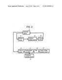
[0015] The following is a more detailed description of the present exemplary embodiment. FIG. 2 is an electrical diagram of an angular velocity sensor as another example of the electronic device. The angular velocity sensor at least includes detection device 21, monitor circuit 41, vibration control circuit 42, and drive circuit 43. Detection device 21 is vibrated by a drive signal outputted from drive circuit 43. Monitor circuit 41 detects and amplifies a monitor signal according to the vibration amplitude from detection device 21. Vibration control circuit 42 receives the monitor signal amplified by monitor circuit 41, and keeps the amplitude of the monitor signal constant, thereby keeping the drive amplitude of detection device 21 constant. Drive circuit 43 receives the constant-amplitude monitor signal from vibration control circuit 42 and outputs the drive signal.
[0016] Detection device 21 detects an angular velocity, which is then detected as a signal by pick up circuit 22. Pick up circuit 22 outputs an output signal to analog-digital converter 23 where the signal is converted into a digital signal. Analog-digital converter 23 outputs an output signal to filter 26 which outputs an output signal to output voltage decision circuit 27.
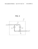
[0017] FIG. 3 is an electrical diagram of filter 26 in the electronic device according to the present exemplary embodiment. First, the output signal of analog-digital converter 23 is supplied to first amplifier 51 having gain a, and delay device 52 having a delay time T. Next, delay device 52 outputs an output signal to second amplifier 53 having gain β. The outputs of first and second amplifiers 51 and 53 are added by adder circuit 54 and then outputted therefrom. Filter 26 in the present exemplary embodiment is a low-pass filter.
[0018] Filter 26 can alternatively be a band-pass filter or a high-pass filter instead of the low-pass filter. It is preferable, however, to use the low-pass filter in order to accurately detect a change, mentioned below, in the integral of an after-mentioned quantization noise level in output voltage decision circuit 27.
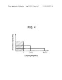
[0019] The AD conversion in analog-digital converter 23 is performed based on a sampling frequency fs which is supplied from frequency variable circuit 25. At this moment, a quantization error occurs according to the value of the sampling frequency fs for the AD conversion, thereby generating quantization noise.
[0020] FIG. 4 shows the relation between the sampling frequency and the quantization noise of the analog-digital converter in the electronic device according to the present exemplary embodiment. The frequency spectrum of the quantization noise changes with the value of the sampling frequency fs. For example, when the sampling frequency is doubled, the quantization noise has twice the frequency range, and the quantization noise level is reduced by half.
[0021] FIG. 5 shows the relation between sampling frequency and quantization noise after the output signal of the analog-digital converter passes through the filter in the electronic device according to the present exemplary embodiment. Frequency variable circuit 25 shown in FIG. 2 changes the sampling frequency fs of analog-digital converter 23 to a frequency outside of the pass band of filter 26. This results in a decrease in the integral of the quantization noise level of the output signal of filter 26 in the pass band as shown in FIG. 5. In other words, the integral of the quantization noise level to be supplied to output voltage decision circuit 27 can be changed by changing the sampling frequency fs by frequency variable circuit 25. In the case of a failure, such as disconnection or the fixation of an output value, in a signal path located after analog-digital converter 23, the integral of the quantization noise level to be supplied to output voltage decision circuit 27 does not change even when the sampling frequency fs is changed. This allows the failure to be determined by calculating the integral of the quantization noise level by output voltage decision circuit 27.
[0022] With this structure, the electronic device has a circuit with a self-diagnosis function without providing a diagnosis signal supply circuit for supplying an analog signal for failure diagnosis. As a result, the circuit of the electronic device can be compact.
[0023] The present exemplary embodiment explains the angular velocity sensor as an example, but the effect of the present invention can also be obtained in other electronic devices, such as acceleration sensors, as long as they are provided with analog-digital converter 23 having a variable sampling frequency.
INDUSTRIAL APPLICABILITY
[0024] An electronic device of the present invention having a compact circuit is useful to various electronic devices, such as automobiles, aircrafts, ships, robots, digital cameras, car navigation systems, and sensors.
Reference Marks in the Drawings
[0025] 1 detection device [0026] 2 pick up circuit [0027] 3 analog-digital converter [0028] 4 frequency supply circuit [0029] 7 output voltage decision circuit [0030] 11 detection device [0031] 12 pick up circuit [0032] 13 analog-digital converter [0033] 15 frequency variable circuit [0034] 16 filter [0035] 17 output voltage decision circuit [0036] 21 detection device [0037] 22 pick up circuit [0038] 23 analog-digital converter [0039] 25 frequency variable circuit [0040] 26 filter [0041] 27 output voltage decision circuit [0042] 41 monitor circuit [0043] 42 vibration control circuit [0044] 43 drive circuit [0045] 51 first amplifier [0046] 52 delay device [0047] 53 second amplifier [0048] 54 adder circuit
User Contributions:
Comment about this patent or add new information about this topic:
Images included with this patent application:
 |  |
 |  |
 |  |
| Similar patent applications: | |
| Date | Title |
|---|---|
| 2008-09-04 | Key system for an electronic device |
| 2008-09-04 | Handheld electronic device and keypad providing enhanced usability and reduced size, and associated method |
| 2008-09-04 | Control method of alterable key and portable electronic device having alterable key |
| 2008-09-11 | Remote control integration device for controlling electronic devices |
| 2008-09-25 | Riser, ridge based touch keypad for portable electronic device |
| New patent applications in this class: | |
| Date | Title |
|---|---|
| 2019-05-16 | Computational devices using thermometer coding and scaling networks on unary encoded data |
| 2019-05-16 | Systems and methods for digital excess loop delay compensation in a continuous time delta sigma modulator |
| 2016-12-29 | Apparatus for overload recovery of an integrator in a sigma-delta modulator |
| 2016-12-29 | Reducing distortion in an analog-to-digital converter |
| 2016-09-01 | Digital-to-analog converter using nonlinear capacitance compensation |
| New patent applications from these inventors: | |
| Date | Title |
|---|---|
| 2022-03-31 | Electromagnetic valve drive device |
| 2022-03-31 | Electromagnetic valve driving device |
| 2022-03-31 | Electromagnetic valve driving device |
| 2012-02-02 | Angular velocity sensor |
| 2012-01-12 | Electronic part and method of detecting faults therein |
| Top Inventors for class "Coded data generation or conversion" | |
| Rank | Inventor's name |
|---|---|
| 1 | Shiro Dosho |
| 2 | Jong Kee Kwon |
| 3 | Kazuo Matsukawa |
| 4 | Young Deuk Jeon |
| 5 | Ahmed Mohamed Abdelatty Ali |