Patent application title: LCD APPARATUS WITH CAMERA MODULE, AND METHOD OF MAKING SAME
Inventors:
Jen-Tsorng Chang (Tu-Cheng, TW)
Assignees:
HON HAI PRECISION INDUSTRY CO., LTD.
IPC8 Class: AH04N5222FI
USPC Class:
34833308
Class name: Camera, system and detail with electronic viewfinder or display monitor including optics
Publication date: 2011-06-23
Patent application number: 20110149139
Abstract:
An exemplary liquid crystal display apparatus includes a liquid crystal
display device and a cameral module. The liquid crystal display device
includes a first glass substrate, a second glass substrate parallel to
the first glass substrate, and a liquid crystal layer formed between the
first glass substrate and the second substrate; and the cameral module
includes a lens, and an image sensor, wherein the image sensor is located
between the first glass substrate and the second glass substrate, and is
separated from the liquid crystal layer, and the lens is located on an
opposite side of the first glass substrate to the image sensor, and an
optical axis of the lens is aligned with a central normal of the image
sensor.Claims:
1. A liquid crystal display apparatus comprising: a liquid crystal
display device comprising a first glass substrate, a second glass
substrate parallel to the first glass substrate, and a liquid crystal
layer formed between the first glass substrate and the second substrate;
and a cameral module comprising a lens, and an image sensor, wherein the
image sensor is located between the first glass substrate and the second
glass substrate, and is separated from the liquid crystal layer, and the
lens is located on an opposite side of the first glass substrate to the
image sensor, and an optical axis of the lens is aligned with a central
normal of the image sensor.
2. The liquid crystal display apparatus according to claim 1, wherein the first glass substrate has a first surface and an opposite second surface parallel to the first surface, the second glass substrate has a third surface and an opposite fourth surface parallel to the third surface, the second surface faces the third surface, the liquid crystal apparatus further has a transparent conductive layer, the transparent conductive layer is disposed between the second surface and the third surface, the image sensor is electrically connected to the transparent conductive layer.
3. The liquid crystal display apparatus according to claim 2, further comprising a printed circuit board, wherein the transparent conductive layer is electrically connected to the printed circuit board, and attached to the second surface or the third surface; and the image sensor is attached to the transparent conductive layer.
4. The liquid crystal display apparatus according to claim 2, wherein the camera module further comprises a barrel located on the first surface, and the lens accommodated inside the barrel.
5. The liquid crystal display apparatus according to claim 2, wherein the lens is arranged on a displaying side of the LCD apparatus.
6. The liquid crystal display apparatus according to claim 2, wherein the lens is arranged on an opposite side of the LCD apparatus to a displaying side thereof.
7. A method of making a liquid crystal display apparatus, comprising: providing a first glass substrate; providing a second glass substrate parallel to the first glass substrate; providing an image sensor; attaching the image sensor onto the first glass substrate; arranging the image sensor between the first and second glass substrates; forming a liquid crystal layer between the first glass substrate and the second substrate; and arranging a lens on an opposite side of the first glass substrate to the image sensor in an manner that an optical axis of the lens is aligned with the central normal of the image sensor.
8. The method according to claim 7, further comprising: attaching a transparent conductive layer to the first glass substrate, and electrically connecting the transparent conductive layer to the image sensor.
9. The method according to claim 7, wherein the lens is embossed on the first glass substrate.
10. The method according to claim 7, further comprising: fixing a barrel on the first glass substrate to accommodate the lens.
Description:
BACKGROUND
[0001] 1. Technical Field
[0002] The present disclosure relates to a liquid crystal display (LCD) apparatus packaged with a camera module, and a method of making the LCD apparatus.
[0003] 2. Description of Related Art
[0004] LCD apparatus are widely used in mobile phones, or personal computers, and camera modules are also applied in these electronic apparatus.
[0005] A typical LCD apparatus and camera module combination is configured with the camera module adjacent to a display of the LCD apparatus which adds to the bulk of the apparatus. What is needed is an LCD apparatus with camera module embedded therein without an independent packaging space.
BRIEF DESCRIPTION OF THE DRAWINGS
[0006] Many aspects of the present LCD apparatus packaged with a camera module can be better understood with reference to the following drawings. The components in the drawings are not necessarily drawn to scale, the emphasis instead being placed upon clearly illustrating the principles of the present, LCD apparatus and method. Moreover, in the drawings, like reference numerals designate corresponding parts throughout the several views.
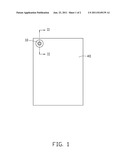
[0007] FIG. 1 is a perspective view of an LCD apparatus in accordance with an exemplary embodiment.
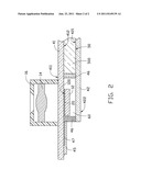
[0008] FIG. 2 is a sectional view in the direction of II-II shown in FIG. 1.
DETAILED DESCRIPTION
[0009] FIG. 1 and FIG. 2 show a liquid crystal display (LCD) apparatus 40 packaged with a camera module 10. The LCD apparatus 40 includes an external first glass substrate 41 laid over a second glass substrate 42 parallel to the first glass substrate 41. The first glass substrate 41 and the second glass substrate 42 need not be the same size. In this embodiment, the first glass substrate 41 overhangs the second glass substrate 42. The first glass substrate 41 has a first surface 411 and an opposite second surface 412 parallel to the first surface 411. The second glass substrate 42 has a third surface 421 and a opposite fourth surface 422 parallel to the third surface 421. The second surface 412 faces the third surface 421. The fourth side 422 is opposite to the displaying side. Some sealing elements 46 are applied to divide the space between the first glass substrate 41 and the second glass substrate 42 into a first closed space 50 and a second closed space 60. The sealing elements 46 can be made of epoxy resin, or atramentous polymer, or glue. The first closed space 50 accommodates liquid crystal 500 to form a liquid crystal layer. The liquid crystal layer defines a display area for the LCD apparatus 10. The second closed space 60 is adjacent to the first glass closed space 50 for a camera module 10 embedded therein.
[0010] The camera module 10 includes an image sensor 12 and a lens 14. The image sensor 12 is accommodated in the second closed space 60. The image sensor 12 has a light sensing surface 120. The lens 14 is located on an opposite side of the first glass substrate 41 to the image sensor 12, for example, the first surface 411, also defining a displaying side in this embodiment. An optical axis of the lens 14 is aligned with a central normal of the image sensor 12. A transparent conductive layer 20 is attached to the second surface 412 or the third surface 421. The image sensor 12 is attached to the transparent conductive layer 20. The transparent conductive layer 20 is configured for electrically connecting the image sensor 12 to some other unit, for example, a printed circuit board (PCB) 45, or a processor of the display apparatus 40. The transparent conductive layer 20 can be made of indium-tin oxide material or the like. The first glass substrate 41 keeps the image sensor 12 from pollution of dust and small particles. Therefore, a cover glass plate (usually appearing in traditional process) covering the image sensor 12 is not necessary.
[0011] The printed circuit board 45 has a number of interdigitated electrodes 47, and the interdigitated electrodes 47 are electrically connected to the transparent conductive layer 20. The printed circuit board 45 may be located adjacent the first glass substrate 41 or the second glass substrate 42.
[0012] The camera module 10 further has a barrel 16 to receive the lens 14 and other possible optical units, such as a filter. The barrel 16 is glued on the first surface 411 of the first glass substrate 41.
[0013] In another embodiment, the lens 14 can be a kind of wafer level packaged lens without a barrel can be directly embossed on the first glass substrate 41. The embossing method, for example, has following steps, first, put transparent material in a liquid or plastically deformable state on the first surface 411 of the first glass substrate 41; second, mold an optical structure, for example, a lens, on the transparent material; third, cure the transparent material with ultraviolet light and remove the mold. Thus, a lens is directly embossed on the first glass substrate 41.
[0014] The lens 14 can be also arranged on an opposite side of the LCD apparatus to the displaying side thereof, for example, the fourth surface 422, to face a different direction when capturing images.
[0015] The camera module 10 is located in a corner region of the LCD display apparatus 40 or other place except the display area of the LCD apparatus 40.
[0016] The camera module 10 can be packaged in the LCD apparatus 40 by following steps.
[0017] First, a first glass substrate 41 and a second glass substrate 42 are provided. The first glass substrate 41 has a first surface 411 and a second surface 412 parallel to the first surface 411. The second glass substrate 42 has a third surface 421 and a second surface 422. The third surface 421 is divided into two parts by some sealing elements 46. One part defines a display area, and the other part defines an area for locating a camera module 10.
[0018] Second, a transparent conductive layer 20 is attached to the second surface 412. An image sensor 12 at the second surface 412 is electrically connected with the transparent conductive layer 20. Alternatively, the transparent conductive layer 20 could be attached to the third surface 421. The image sensor 12 at the third surface 412 could be electrically connected with the transparent conductive layer 20. The transparent conductive layer 20 could also be attached to the second surface 412, and the image sensor 12 is arranged at the third surface 421. It is possible that the transparent conductive layer 20 is attached to the third surface 421, and the image sensor 12 is located at the second surface 412.
[0019] Third, the first glass substrate 41 is arranged on the second glass substrate 42. Because the first glass substrate 41 can contact with the sealing elements 46, a first closed space 50 and a second closed space 60 are formed between the first glass substrate 41 and the second glass substrate 42.
[0020] Fourth, liquid crystal 500 is introduced into the first closed space 50 to form a liquid crystal layer. The transparent conductive layer 20 is electrically connected to a printed circuit board 45 through some interdigitated electrodes 47. Now the image sensor 12 is located inside the second closed space 60.
[0021] Fifth, a lens 14 is arranged on the first surface 411 of the first glass substrate 41. An optical axis of the lens 14 is aligned with the central normal of the image sensor 12. Besides the lens 14, a barrel 16 can be also glued on the first surface 411, and the lens 14 is placed inside the barrel 16.
[0022] In another alternative embodiment, the lens 14 can be embossed on the first glass substrate 41 without any barrel.
[0023] The camera module 10 employs the first glass substrate 41 as a glass cover plate to keep the image sensor 12 from pollution of dust or small particles, so the number of elements needed during the packaging process decreases. Because the camera module 10 is embedded in the LCD apparatus 40 with the image sensor 12 covered by one glass substrate of the LCD apparatus 40, an independent packaging space, such as a frame, is not needed, the packaging volume decreases. Or the frame surrounds the LCD apparatus 40 can be narrower than before, thus the display area seems bigger.
[0024] It is understood that the above-described embodiments are intended to illustrate rather than limit the disclosure. Variations may be made to the embodiments without departing from the spirit of the disclosure. Accordingly, it is appropriate that the appended claims be construed broadly and in a manner consistent with the scope of the disclosure.
User Contributions:
Comment about this patent or add new information about this topic:
Images included with this patent application:
 |  |
| New patent applications in this class: | |
| Date | Title |
|---|---|
| 2016-02-04 | Display device, display control method, and non-transitory recording medium |
| 2015-12-31 | Image processing device, imaging device, program, and image processing method |
| 2015-12-24 | Image pickup apparatus and control method |
| 2015-05-28 | Image focusing |
| 2015-05-14 | Camera and method of controlling operation of same |
| New patent applications from these inventors: | |
| Date | Title |
|---|---|
| 2016-04-21 | Touch pen and electronic device having the same |
| 2016-03-31 | Display device with sound generation regions having different areas |
| 2016-03-10 | Encapsulation structure and method for making same |
| 2015-07-16 | Suppporting device, method for manufacturing thin film transistor array substrate and method for manufacturing liquid crystal display |
| 2015-06-04 | Light guide plate and backlight module having same |
| Top Inventors for class "Television" | |
| Rank | Inventor's name |
|---|---|
| 1 | Canon Kabushiki Kaisha |
| 2 | Kia Silverbrook |
| 3 | Peter Corcoran |
| 4 | Petronel Bigioi |
| 5 | Eran Steinberg |