Patent application title: HEAT SINK AND MOTHERBOARD ASSEMBLY UTILIZING THE HEAT SINK
Inventors:
Zheng-Heng Sun (Tu-Cheng, TW)
Assignees:
HON HAI PRECISION INDUSTRY CO., LTD.
IPC8 Class: AH05K720FI
USPC Class:
361704
Class name: For electronic systems and devices with cooling means thermal conduction
Publication date: 2010-09-30
Patent application number: 20100246131
ng heat for a motherboard, includes a package
portion, a heat dissipating device made of heat conducting material, and
a number of grounding pins made of heat conducting material. The package
portion includes a top wall. The heat dissipating device is exposed out
of the top wall of the package portion. The number of grounding pins
extending down through the package portion, to be soldered to a number of
bonding grounding pads of a corresponding idle chip installing area of
the motherboard, respectively. Top portions of the grounding pins contact
the heat dissipating device. A motherboard assembly utilizing the heat
sink is also disclosed.Claims:
1. A heat sink for dissipating heat for a motherboard, the heat sink
comprising:a package portion comprising a top wall;a heat dissipating
device made of heat conducting material, the heat dissipating device
being exposed out of the top wall of the package portion; anda plurality
of grounding pins made of heat conducting material, the plurality of
grounding pins extending down through the package portion, to be soldered
to a plurality of bonding grounding pads of a corresponding chip
installing area of the motherboard, wherein top portions of the plurality
of grounding pins contact the heat dissipating device.
2. The heat sink of claim 1, wherein the plurality of grounding pins are integrally formed from the heat dissipating device.
3. The heat sink of claim 1, wherein the package portion is made of insulating material.
4. The heat sink of claim 1, further comprising a plurality of supporting pins, wherein the plurality of supporting pins extend down through the package portion, to be supported on a plurality of bonding non-grounding pads of the corresponding chip installing area of the motherboard.
5. The heat sink of claim 4, wherein the plurality of supporting pins do not contact the heat dissipating device.
6. The heat sink of claim 4, wherein the package portion further comprises four sidewalls connected to the top wall, the plurality of grounding pins and the plurality of supporting pins extend down from the sidewalls of the package portion.
7. A motherboard assembly comprising:a motherboard comprising an idle chip installing area, the idle chip installing area comprising a plurality of bonding grounding pads; anda heat sink comprising a package portion, a heat dissipating device exposed out of a top of the package portion, and a plurality of grounding pins contacting the heat dissipating device and extending down through the package portion, wherein the heat dissipating device and the plurality of grounding pins are made of heat conducting material, the plurality of grounding pins are soldered to the plurality of bonding grounding pads, respectively.
8. The motherboard assembly of claim 7, wherein the plurality of grounding pins are integrally formed from the heat dissipating device.
9. The motherboard assembly of claim 7, wherein the package portion is made of insulating material.
10. The motherboard assembly of claim 7, wherein the idle chip installing area further comprises a plurality of bonding non-grounding pads, the heat sink further comprises a plurality of supporting pins extending down through the package portion and supported on the plurality of bonding non-grounding pads, respectively, the plurality of supporting pins do not contact the heat dissipating device.
11. The motherboard assembly of claim 10, wherein the package portion further comprises four sidewalls connected to the top wall, the plurality of supporting pins extend down from the sidewalls of the package portion.
12. The motherboard assembly of claim 10, wherein a shape of the heat sink is the same as that of a chip which can be installed on the idle chip installing area of the motherboard; structures and arrangements of the grounding pins and the supporting pins extending down from the package portion are the same as those of grounding pins and non-grounding pins of the corresponding chip.Description:
CROSS-REFERENCE TO RELATED APPLICATION
[0001]The present application is related to a co-pending U.S. patent application (Attorney Docket No. US24163) filed on the same date and having the same title with the present application, which is assigned to the same assignee with this patent application.
BACKGROUND
[0002]1. Technical Field
[0003]The present disclosure relates to a heat sink and a motherboard assembly utilizing the heat sink.
[0004]2. Description of Related Art
[0005]An electronic device, such as a computer, usually includes a fan and a heat sink installed on a heat generating component of a motherboard for dissipating heat. However, some of the heat produced by the heat generating component will be transferred to the motherboard through pins of the heat generating component, which will lead to undesirable increase of the temperature of the motherboard.
BRIEF DESCRIPTION OF THE DRAWINGS
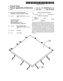
[0006]FIG. 1 is an exploded, isometric view of an embodiment of a heat sink together with a motherboard, the heat sink including a heat dissipating device, a plurality of grounding pins and a plurality of supporting pins.
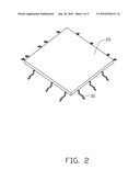
[0007]FIG. 2 is an isometric view of the heat dissipating device and the plurality of grounding pins of FIG. 1.
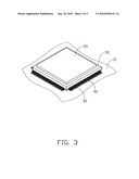
[0008]FIG. 3 is an assembled, isometric view of FIG. 1.
DETAILED DESCRIPTION
[0009]Referring to FIGS. 1 and 2, an embodiment of a heat sink 1 for dissipating heat for a motherboard 10, includes a heat dissipating device 20, a plurality of grounding pins 30, a plurality of supporting pins 40, and a package portion 50 made of insulating material. The package portion 50 includes a top wall 51, and four sidewalls 52 perpendicularly connected to the top wall 51.
[0010]The motherboard 10 includes an idle chip installing area 14. The idle chip installing area 14 includes a plurality of bonding pads 15. Some of the bonding pads 15 are bonding grounding pads 151 connected to a grounding layer of the motherboard 10, and the others of the bonding pads 15 are bonding non-grounding pads 152.
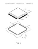
[0011]The heat dissipating device 20 and the plurality of grounding pins 30 are made of heat conducting material. The plurality of grounding pins 30 are integrally formed from the heat dissipating device 20, corresponding to the bonding grounding pads 151 of the idle chip installing area 14 of the motherboard 10. The heat dissipating device 20, the plurality of grounding pins 30, the plurality of supporting pins 40, and the package portion 50 are packaged to form the heat sink 1. After packaging, the heat dissipating device 20 is exposed out of the top wall 51 of the package portion 50; the plurality of grounding pins 30 and the plurality of supporting pins 40 are exposed out of and extending down from the sidewalls 52 of the package portion 50, corresponding to the bonding grounding pads 151 and the bonding non-grounding pads 152, respectively. The plurality of supporting pins 40 do not contact the heat dissipating device 20. A shape of the heat sink 1 is the same as that of a chip which can be otherwise installed on the idle chip installing area 14 of the motherboard 10; structures and arrangements of the plurality of grounding pins 30 and the plurality of supporting pins 40 are the same as those of the grounding pins and non-grounding pins of the corresponding chip.
[0012]Referring to FIG. 3, in use, the heat sink 1 is placed on the idle chip installing area 14 of the motherboard 10 to allow the plurality of grounding pins 30 and the plurality of supporting pins 40 to contact the bonding grounding pads 151 and the bonding non-grounding pads 152 of the idle chip installing area 14, respectively. The plurality of grounding pins 30 and the plurality of supporting pins 40 are soldered to the bonding grounding pads 151 and the bonding non-grounding pads 152, respectively. Thereby, the heat sink 1 is mounted on the idle chip installing area 14 of the motherboard 10. Heat from the motherboard 90 is transferred to the heat dissipating device 20 through the grounding pins 30, and then is dissipated to the air through the heat dissipating device 20. Therefore, temperature of the motherboard 10 can be kept low. Because the heat sink 1 is mounted on the idle chip installing area 14 of the motherboard 10, which means the heat sink 1 does not occupy other space of the motherboard 10, the heat sink 1 will not influence installation of other electronic components.
[0013]It is to be understood, however, that even though numerous characteristics and advantages of the present disclosure have been set forth in the foregoing description, together with details of the structure and function of the disclosure, the disclosure is illustrative only, and changes may be made in details, especially in matters of shape, size, and arrangement of parts within the principles of the disclosure to the full extent indicated by the broad general meaning of the terms in which the appended claims are expressed.
Claims:
1. A heat sink for dissipating heat for a motherboard, the heat sink
comprising:a package portion comprising a top wall;a heat dissipating
device made of heat conducting material, the heat dissipating device
being exposed out of the top wall of the package portion; anda plurality
of grounding pins made of heat conducting material, the plurality of
grounding pins extending down through the package portion, to be soldered
to a plurality of bonding grounding pads of a corresponding chip
installing area of the motherboard, wherein top portions of the plurality
of grounding pins contact the heat dissipating device.
2. The heat sink of claim 1, wherein the plurality of grounding pins are integrally formed from the heat dissipating device.
3. The heat sink of claim 1, wherein the package portion is made of insulating material.
4. The heat sink of claim 1, further comprising a plurality of supporting pins, wherein the plurality of supporting pins extend down through the package portion, to be supported on a plurality of bonding non-grounding pads of the corresponding chip installing area of the motherboard.
5. The heat sink of claim 4, wherein the plurality of supporting pins do not contact the heat dissipating device.
6. The heat sink of claim 4, wherein the package portion further comprises four sidewalls connected to the top wall, the plurality of grounding pins and the plurality of supporting pins extend down from the sidewalls of the package portion.
7. A motherboard assembly comprising:a motherboard comprising an idle chip installing area, the idle chip installing area comprising a plurality of bonding grounding pads; anda heat sink comprising a package portion, a heat dissipating device exposed out of a top of the package portion, and a plurality of grounding pins contacting the heat dissipating device and extending down through the package portion, wherein the heat dissipating device and the plurality of grounding pins are made of heat conducting material, the plurality of grounding pins are soldered to the plurality of bonding grounding pads, respectively.
8. The motherboard assembly of claim 7, wherein the plurality of grounding pins are integrally formed from the heat dissipating device.
9. The motherboard assembly of claim 7, wherein the package portion is made of insulating material.
10. The motherboard assembly of claim 7, wherein the idle chip installing area further comprises a plurality of bonding non-grounding pads, the heat sink further comprises a plurality of supporting pins extending down through the package portion and supported on the plurality of bonding non-grounding pads, respectively, the plurality of supporting pins do not contact the heat dissipating device.
11. The motherboard assembly of claim 10, wherein the package portion further comprises four sidewalls connected to the top wall, the plurality of supporting pins extend down from the sidewalls of the package portion.
12. The motherboard assembly of claim 10, wherein a shape of the heat sink is the same as that of a chip which can be installed on the idle chip installing area of the motherboard; structures and arrangements of the grounding pins and the supporting pins extending down from the package portion are the same as those of grounding pins and non-grounding pins of the corresponding chip.
Description:
CROSS-REFERENCE TO RELATED APPLICATION
[0001]The present application is related to a co-pending U.S. patent application (Attorney Docket No. US24163) filed on the same date and having the same title with the present application, which is assigned to the same assignee with this patent application.
BACKGROUND
[0002]1. Technical Field
[0003]The present disclosure relates to a heat sink and a motherboard assembly utilizing the heat sink.
[0004]2. Description of Related Art
[0005]An electronic device, such as a computer, usually includes a fan and a heat sink installed on a heat generating component of a motherboard for dissipating heat. However, some of the heat produced by the heat generating component will be transferred to the motherboard through pins of the heat generating component, which will lead to undesirable increase of the temperature of the motherboard.
BRIEF DESCRIPTION OF THE DRAWINGS
[0006]FIG. 1 is an exploded, isometric view of an embodiment of a heat sink together with a motherboard, the heat sink including a heat dissipating device, a plurality of grounding pins and a plurality of supporting pins.
[0007]FIG. 2 is an isometric view of the heat dissipating device and the plurality of grounding pins of FIG. 1.
[0008]FIG. 3 is an assembled, isometric view of FIG. 1.
DETAILED DESCRIPTION
[0009]Referring to FIGS. 1 and 2, an embodiment of a heat sink 1 for dissipating heat for a motherboard 10, includes a heat dissipating device 20, a plurality of grounding pins 30, a plurality of supporting pins 40, and a package portion 50 made of insulating material. The package portion 50 includes a top wall 51, and four sidewalls 52 perpendicularly connected to the top wall 51.
[0010]The motherboard 10 includes an idle chip installing area 14. The idle chip installing area 14 includes a plurality of bonding pads 15. Some of the bonding pads 15 are bonding grounding pads 151 connected to a grounding layer of the motherboard 10, and the others of the bonding pads 15 are bonding non-grounding pads 152.
[0011]The heat dissipating device 20 and the plurality of grounding pins 30 are made of heat conducting material. The plurality of grounding pins 30 are integrally formed from the heat dissipating device 20, corresponding to the bonding grounding pads 151 of the idle chip installing area 14 of the motherboard 10. The heat dissipating device 20, the plurality of grounding pins 30, the plurality of supporting pins 40, and the package portion 50 are packaged to form the heat sink 1. After packaging, the heat dissipating device 20 is exposed out of the top wall 51 of the package portion 50; the plurality of grounding pins 30 and the plurality of supporting pins 40 are exposed out of and extending down from the sidewalls 52 of the package portion 50, corresponding to the bonding grounding pads 151 and the bonding non-grounding pads 152, respectively. The plurality of supporting pins 40 do not contact the heat dissipating device 20. A shape of the heat sink 1 is the same as that of a chip which can be otherwise installed on the idle chip installing area 14 of the motherboard 10; structures and arrangements of the plurality of grounding pins 30 and the plurality of supporting pins 40 are the same as those of the grounding pins and non-grounding pins of the corresponding chip.
[0012]Referring to FIG. 3, in use, the heat sink 1 is placed on the idle chip installing area 14 of the motherboard 10 to allow the plurality of grounding pins 30 and the plurality of supporting pins 40 to contact the bonding grounding pads 151 and the bonding non-grounding pads 152 of the idle chip installing area 14, respectively. The plurality of grounding pins 30 and the plurality of supporting pins 40 are soldered to the bonding grounding pads 151 and the bonding non-grounding pads 152, respectively. Thereby, the heat sink 1 is mounted on the idle chip installing area 14 of the motherboard 10. Heat from the motherboard 90 is transferred to the heat dissipating device 20 through the grounding pins 30, and then is dissipated to the air through the heat dissipating device 20. Therefore, temperature of the motherboard 10 can be kept low. Because the heat sink 1 is mounted on the idle chip installing area 14 of the motherboard 10, which means the heat sink 1 does not occupy other space of the motherboard 10, the heat sink 1 will not influence installation of other electronic components.
[0013]It is to be understood, however, that even though numerous characteristics and advantages of the present disclosure have been set forth in the foregoing description, together with details of the structure and function of the disclosure, the disclosure is illustrative only, and changes may be made in details, especially in matters of shape, size, and arrangement of parts within the principles of the disclosure to the full extent indicated by the broad general meaning of the terms in which the appended claims are expressed.
User Contributions:
Comment about this patent or add new information about this topic:
Images included with this patent application:
 |  |
 |  |
| Similar patent applications: | |
| Date | Title |
|---|---|
| 2012-03-22 | Printed circuit board, printed circuit board assembly sheet and method of manufacturing the same |
| 2011-12-08 | Expansion card assembly and heat sink thereof |
| 2009-03-26 | Heat sink and cooling unit using the same |
| 2011-07-28 | Hinge and collapsible device utilizing the same |
| 2009-05-07 | Keyboard and keyboard assembling method |
| New patent applications in this class: | |
| Date | Title |
|---|---|
| 2022-05-05 | Aerothermal ring structures providing rf isolation |
| 2016-05-12 | System for controlling industrial and domestic devices |
| 2016-03-24 | Heat dissipation structure, fabricating method, and electronic apparatus |
| 2016-03-10 | Heat dissipation structure for electronic device |
| 2016-03-03 | Curved display and electronic device including the same |
| New patent applications from these inventors: | |
| Date | Title |
|---|---|
| 2014-05-01 | Fan device |
| 2014-03-27 | Mounting device for hard disk drive |
| 2014-02-27 | Electronic device with fan module |
| 2014-01-09 | Front panel assembly with identification plate |
| 2013-12-26 | Electronic device and expansion card of the same |
| Top Inventors for class "Electricity: electrical systems and devices" | |
| Rank | Inventor's name |
|---|---|
| 1 | Zheng-Heng Sun |
| 2 | Levi A. Campbell |
| 3 | Li-Ping Chen |
| 4 | Robert E. Simons |
| 5 | Richard C. Chu |