Patent application title: ELECTRONIC CIRCUIT DEVICE
Inventors:
Susumu Kumakura (Tokyo, JP)
Assignees:
CANON KABUSHIKI KAISHA
IPC8 Class: AH05K114FI
USPC Class:
174261
Class name: Conduits, cables or conductors preformed panel circuit arrangement (e.g., printed circuit) with particular conductive connection (e.g., crossover)
Publication date: 2010-04-08
Patent application number: 20100084177
circuit device in which the bonding state of
electrodes can be detected easily with high precision. The electronic
circuit device has a stack structure in which a plurality of electronic
circuit boards (1a, 1b, 100a, 100b, 100c) are stacked in three or more
layers through ball electrodes (10a, 10b, 20a, 20b) bonded to electrode
pads (30a, 30b, 40b, 50a, 60a), wherein the electrode pads are disposed
such that transmission shaded images of a pair of the electrode pads
provided between adjacent layers partially overlap each other and have a
non-overlapping region in which the transmission shaded images of the
pair of electrode pads are free from overlapping and such that the
transmission shaded image of the non-overlapping region is at least
partially free from overlapping with transmission shaded images of all
the other electrode pads.Claims:
1. An electronic circuit device having a stack structure in which a
plurality of electronic circuit boards are stacked in three or more
layers through ball electrodes bonded to electrode pads,wherein the
electrode pads are disposed such that transmission shaded images of a
pair of the electrode pads provided between adjacent layers partially
overlap each other and have a non-overlapping region in which the
transmission shaded images of the pair of electrode pads are free from
overlapping and such that the transmission shaded image of the
non-overlapping region is at least partially free from overlapping with
transmission shaded images of all the other electrode pads.
2. The electronic circuit device according to claim 1, wherein the electrode pads provided in the different layers each has a protrusion and are disposed such that the protrusions are partly free from overlapping.
3. The electronic circuit device according to claim 1, wherein each of the electrode pads partially overlaps all the other electrode pads provided at corresponding locations of the respective layers.Description:
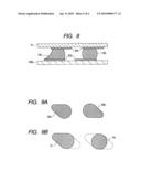
TECHNICAL FIELD
[0001]The present invention relates to an electronic circuit device having a semiconductor package and a printed wiring board which are connected to each other through intermediation of ball electrodes, and a stack structure in which a plurality of printed wiring boards are stacked together through intermediation of ball electrodes, which is capable of detecting the connection state of ball electrodes with ease and high precision.
BACKGROUND ART
[0002]In recent years, there can be seen advancement in the density increase of an electronic circuit device, and an attention is paid onto an electronic circuit device, in which a plurality of ball electrodes are arranged in a peripheral configuration or an array configuration to connect a semiconductor package and a printed wiring board.
[0003]However, it is difficult to visually confirm the connection state of ball electrodes that are disposed between the semiconductor package and the printed wiring board from outside.
[0004]For that reason, as a method of confirming the connection state of ball electrodes, there is known a method of applying a feature including a recess or intrusion to the shape of a pad to which a ball electrode is to be connected and determining the connection state based on the shape of a shaded image (transmission shaded image) of the ball electrode obtained by x-ray transmission (or x-ray fluoroscopy) (see Japanese Patent Application Laid-Open No. H09-219583 and Japanese Patent No. 3601714).
[0005]Further, there is also known a technology of making different from each other the shapes in which an electrode pad provided on a lower surface of an electronic circuit board and a foot pattern provided on an upper surface of a board are connected through intermediation of a ball electrode to easily confirm the connection state between the upper and lower members by one-time x-ray inspection (Japanese Patent Application Laid-Open No. H09-051017).
[0006]However, in recent years, in order to further advance density increase, attention is paid to an electronic circuit device in which a semiconductor package and a printed wiring board which are connected by ball electrodes are not disposed in a planar configuration as in the conventional art, but are stacked in three or more layers.
[0007]In such an electronic circuit board, because the shaded images obtained by transmission of ball electrodes that are disposed in a stacked fashion are displayed in a superimposed manner, there is still an unsolved problem that the connection state of the ball electrodes cannot easily be confirmed by the above-mentioned procedure.
[0008]Also, in the electronic circuit device having the stack structure, it is difficult to radiate a heat generated in the electronic circuit device to outside as compared to the conventional electronic circuit device having the planar arrangement. Therefore, the electronic circuit device needs to have such a stack structure as to efficiently radiate heat to outside. In general, the ball electrode is smaller in thermal conductivity than other members and therefore serves as a good radiation path.
[0009]However, in order to image the connection state of the ball electrodes by x-ray inspection, when the electrode pads and the ball electrodes which are provided in different layers are disposed in a nested manner, a heat generated in the semiconductor package or the printed wiring board needs to excessively pass through the board, with the result that the heat generated in the interior of the stack structure is difficult to be radiated to outside.
DISCLOSURE OF THE INVENTION
[0010]The present invention has been accomplished in view of the above problems, and it is, therefore, an object of the present invention to provide an electronic circuit device having a structure in which a heat generated in a stack structure is efficiently radiated and is capable of detecting, by a simple method, a connection failure of ball electrodes in the stack structure in which a plurality of semiconductor packages and a plurality of printed wiring boards are stacked together.
[0011]The present invention provides an electronic circuit device having a stack structure in which a plurality of electronic circuit boards are stacked in three or more layers through ball electrodes bonded to electrode pads,
[0012]wherein the electrode pads are disposed such that transmission shaded images of a pair of the electrode pads provided between adjacent layers partially overlap each other and have a non-overlapping region in which the transmission shaded images of the pair of electrode pads are free from overlapping and such that the transmission shaded image of the non-overlapping region is at least partially free from overlapping with transmission shaded images of all the other electrode pads.
[0013]In the present invention, it is preferred that the electrode pads provided in the different layers each has a protrusion and are disposed such that the protrusions are partly free from overlapping.
[0014]Furthermore, it is also preferred that each of the electrode pads partially overlaps all the other electrode pads provided at corresponding locations in the layer (or board) stacking direction of the respective layers, which is advantageous for attaining the efficient heat radiation.
[0015]By adopting such a configuration, the radiation path can be shortened, so that efficient radiation can be achieved, and the connection state of the ball electrodes in the stack structure can be visually confirmed easily by means of the shapes of the transmission shaded images.
[0016]Further features of the present invention will become apparent from the following description of exemplary embodiments with reference to the attached drawings.
BRIEF DESCRIPTION OF THE DRAWINGS
[0017]FIG. 1 is a cross-sectional view illustrating an electronic circuit device according to an embodiment of the present invention;
[0018]FIG. 2 is an enlarged cross-sectional view illustrating a portion of the electronic circuit device of FIG. 1;
[0019]FIGS. 3A and 3B are views illustrating electrode pads of FIG. 2 and shaded images thereof;
[0020]FIG. 4 is an enlarged cross-sectional view illustrating a portion of the electronic circuit device of FIG. 1;
[0021]FIGS. 5A and 5B are views illustrating electrode pads of FIG. 4 and the shaded images thereof;
[0022]FIG. 6 is an enlarged cross-sectional view illustrating a portion of the electronic circuit device of FIG. 1;
[0023]FIGS. 7A and 7B are views illustrating electrode pads of FIG. 6 and shaded images thereof;
[0024]FIG. 8 is an enlarged cross-sectional view illustrating a portion of the electronic circuit device of FIG. 1;
[0025]FIGS. 9A and 9B are views illustrating electrode pads of FIG. 8 and shaded images thereof; and
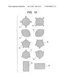
[0026]FIG. 10 is a view illustrating examples of modified shapes of an electrode pad.
BEST MODE FOR CARRYING OUT THE INVENTION
[0027]Preferred embodiments of the present invention will now be described in detail with reference to the accompanying drawings.
[0028]As illustrated in FIG. 1, a first semiconductor package 1a and a first printed wiring board 100a are connected to each other by a plurality of ball electrodes 10a, and a second semiconductor package 1b and a second printed wiring board 100b are connected to each other by a plurality of ball electrodes 10b. A third printed wiring plate 100c and the first printed wiring board 100a are stacked together through intermediation of ball electrodes 20a. Further, the first printed wiring board 100a and the second printed wiring board 100b are stacked together through intermediation of ball electrodes 20b. That is, electronic circuit boards such as semiconductor packages or printed wiring boards are stacked together in a multi-layer structure, and the respective layers are connected to each other through intermediation of ball electrodes.
[0029]In the electronic circuit device having the above stack structure, the ball electrodes 10a are connected to the printed wiring board 100a through intermediation of electrode pads 30a that are disposed on the printed wiring board 100a, and each of the electrode pads 30a has a protrusion in a surface direction of the printed wiring board 100a. Incidentally, the term "surface direction of a printed wiring board" herein employed refers to a direction parallel to the surface of the printed wiring board. That is, it is intended to mean that the cross-sectional shape of the electrode pad 30a taken along a plane parallel to the surface of the printed wiring board 100a is not circular, but has a protruding portion in at least a part of a circle. The ball electrodes 10b are connected to the printed wiring board 100b through intermediation of electrode pads 30b that are disposed on the printed wiring board 100b, and each of the electrode pads 30b has a protrusion in the surface direction of the printed wiring board 100b. Then, the electrode pads 30a and the electrode pads 30b are disposed such that transmission shaded images obtained by transmission of the electrode pads 30a and the electrode pads 30b do not overlap each other at least partially in the protruding portions of the respective electrode pads 30a and 30b.
[0030]Further, the ball electrodes 20b are connected to the printed wiring board 100a through intermediation of electrode pads 50a that are disposed on the printed wiring board 100a, and each of the electrode pads 50a has a portion protruding in the surface direction of the printed wiring board 100a. Then, the electrode pads 30b and the electrode pads 50a are disposed such that transmission shaded images obtained by transmission of the electrode pads 30b and the electrode pads 50a do not overlap each other at least partially in the protruding portions of the respective electrode pads 30b and 50a.
[0031]Further, the ball electrodes 10b are connected to the semiconductor package 1b through intermediation of electrode pads 40b that are disposed on the semiconductor package 1b, and each of the electrode pads 40b has a portion protruding in the surface direction of the semiconductor package 1b. Then, the electrode pads 30b and the electrode pads 40b are disposed such that transmission shaded images obtained by transmission of the electrode pads 30b and the electrode pads 40b do not overlap each other at least partially in the protruding portions of the respective electrode pads 30b and 40b.
[0032]The ball electrodes 20a on a rear surface of the printed wiring board 100a which is on a side opposite to a front surface side on which the ball electrodes 20b are disposed are connected to the printed wiring board 100a through intermediation of electrode pads 60a that are disposed on the printed wiring board 100a. Each of the electrode pads 60a has a portion protruding in the surface direction of the printed wiring board 100a. Then, the electrode pads 50a and the electrode pads 60a are disposed such that transmission shaded images obtained by transmission of the electrode pads 50a and the electrode pads 60a do not overlap each other at least partially in the protruding portions of the respective electrode pads 50a and 60a.
[0033]The electrode pads 30a, 30b, 40a, and 40b have the same diameter and the same axis. Also, the electrode pads 50a and 60a have the same diameter and are coaxial.
[0034]As described above, the semiconductor package 1a is mounted on the printed wiring board 100a through intermediation of the ball electrodes 10a, and the semiconductor package 1b is mounted on the printed wiring board 100b through intermediation of the ball electrodes 10b. Also, the printed wiring boards 100a and 100b are connected to each other by the ball electrodes 20b, and the printed wiring boards 100a and 100c are connected to each other by the ball electrodes 20a.
[0035]Further, the ball electrodes 10b and the ball electrodes 10a that are positioned immediately below the ball electrodes 10b have the same outer diameter (the same diameter) and the same central axis (being coaxial). The ball electrodes 20b and the ball electrodes 20a that are positioned immediately below the ball electrodes 20b have the same outer diameter (the same diameter) and the same central axis (being coaxial). With the above arrangement of the ball electrodes, heat is liable to be transferred through the ball electrodes that are smaller in thermal resistance among the members which constitute the electronic circuit device, which is advantageous in heat radiation. However, there is no limit of the arrangement of the ball electrodes so far as it does not deviate from the spirit of the present invention. That is, it is only necessary that the ball electrodes which are disposed in the different layers overlap each other in a part and do not overlap each other in another part.
[0036]FIG. 2 is an enlarged cross-sectional view illustrating an area including the ball electrodes 10b and the ball electrodes 10a that are positioned immediately below the ball electrodes 10b which is a part of the electronic circuit device illustrated in FIG. 1.
[0037]FIG. 3A illustrates a planar shape in the printed wiring board 100a surface direction of the electrode pads 30a to which the ball electrodes 10a are connected in FIG. 2, and a planar shape in the printed wiring board 100b surface direction of the electrode pads 30b to which the ball electrodes 10b are connected in FIG. 2. Further, FIG. 3B illustrates shaded image through transmission (transmission shaded image) obtained by transmission of the ball electrodes 10b and the ball electrodes 10a shown in FIG. 2.
[0038]The ball electrode 10b at the left side of FIG. 2 is bonded to the electrode pad 30b in a state where the ball electrode 10b fully extends over the protruding portion of the electrode pad 30b. On the other hand, the ball electrode 10a is bonded to the electrode pad 30a in a state where the ball electrode 10a does not extend over the protruding portion of the electrode pad 30a. A shaded image E1 is obtained by transmission of the ball electrodes 10a and 10b in this state. The ball electrode 10b at the right side of FIG. 2 is bonded to the electrode pad 30b in a state where the ball electrode 10b does not extend over the protruding portion of the electrode pad 30b. On the other hand, the ball electrode 10a is bonded to the electrode pad 30a in a state where the ball electrode 10a does not extend over the protruding portion of the electrode pad 30a. A shaded image E2 is obtained by transmission of the ball electrodes 10a and 10b in this state.
[0039]As illustrated in FIG. 3A, the electrode pad 30a to which the ball electrode 10a is connected and the electrode pad 30b to which the ball electrode 10b is connected are each allowed to have a tear drop shaped cross section taken along a plane parallel to the printed wiring board in which a protruding portion is added to a circle. For that reason, by determining a difference in shape of the shaded images E1 and E2 by use of an x-ray inspection apparatus, the bonding state of the ball electrode 10a to the electrode pad 30a and the bonding state of the ball electrode 10b to the electrode pad 30b can easily be detected.
[0040]For example, the determination of the quality of the bonding state can be determined such that when the circularity of the shaded image (E1, E2) is equal to or more than 30% of the outer diameter of the ball electrode (10a, 10b) prior to the bonding to the electrode pad (30a, 30b), the bonding state is determined to be good, while when the circularity of the shaded image (E1, E2) is less than 30% of the outer diameter of the ball electrode (10a, 10b) prior to the bonding to the electrode pad (30a, 30b), the bonding state is determined to be defective. However, the criteria for the determination of the quality can be set depending on the material of the ball electrode to be used or the intended use of the electronic circuit device.
[0041]FIG. 4 is an enlarged cross-sectional view illustrating an area including the ball electrodes 10b and the ball electrodes 20b that are positioned immediately below the ball electrodes 10b.
[0042]FIG. 5A illustrates a planar shape in the printed wiring board 100a surface direction of the electrode pads 30a to which the ball electrodes 10a are connected in FIG. 4, and a planar shape in the printed wiring board 100b surface direction of the electrode pads 30b to which the ball electrodes 10b are connected in FIG. 4. Further, FIG. 5B illustrates shaded image through transmission (transmission shaded image) obtained by transmission of the ball electrodes 10b and the ball electrodes 20b shown in FIG. 4.
[0043]The ball electrode 10b at the left side of FIG. 4 is bonded to the electrode pad 30b in a state where the ball electrode 10b fully extends over the protruding portion of the electrode pad 30b. Further, the ball electrode 20b is bonded to the electrode pad 50a in a state where the ball electrode 20b fully extends over the electrode pad 50a including the protruding portion thereof. A shaded image E3 is obtained by transmission of the ball electrodes 10b and 20b in this state. The ball electrode 10b at the right side of FIG. 4 is bonded to the electrode pad 30b in a state where the ball electrode 10b does not extend over the protruding portion of the electrode pad 30b. Further, the ball electrode 20b is bonded to the electrode pad 50a in a state where the ball electrode 20b fully extends over the electrode pad 50a. A shaded image E4 is obtained by transmission of the ball electrodes 10b and 20b in this state.
[0044]As illustrated in FIG. 5A, the electrode pad 30b to which the ball electrode 10b is connected and the electrode pad 50a to which the ball electrode 20b is connected are each allowed to have a tear drop shaped cross section in which a protruding portion is added to a circle. For that reason, by determining a difference in shape of the shaded images E3 and E4 by use of an x-ray inspection apparatus, the bonding state of the ball electrode 10b to the electrode pad 30a and the bonding state of the ball electrode 20b to the electrode pad 50a can easily be detected.
[0045]FIG. 6 is an enlarged cross-sectional view illustrating an area including the ball electrodes 20b and the ball electrodes 20a that are positioned immediately below the ball electrodes 20b.
[0046]FIG. 7A illustrates a planar shape in the printed wiring board 100a surface direction of the electrode pads 50a to which the ball electrodes 20b are connected in FIG. 6, and a planar shape in the printed wiring board 100b surface direction of the electrode pads 60a to which the ball electrodes 20a are connected in FIG. 6. Further, FIG. 7B illustrates shaded image through transmission (transmission shaded image) obtained by transmission of the ball electrodes 20b and the ball electrodes 20a shown in FIG. 4.
[0047]The ball electrode 20b at the left side of FIG. 6 is bonded to the electrode pad 50a in a state where the ball electrode 10b fully extends over the protruding portion of the electrode pad 50a. Further, the ball electrode 20a is bonded to the electrode pad 60a in a state where the ball electrode 20a does not extend over the protruding portion of the electrode pad 60a. A shaded image E5 is obtained by transmission of the ball electrodes 20b and 20a in this state. The ball electrode 20b at the right side of FIG. 6 is bonded to the electrode pad 50a in a state where the ball electrode 20b does not extend over the protruding portion of the electrode pad 50a. Further, the ball electrode 20a is bonded to the electrode pad 60a in a state where the ball electrode 20a does not extend over the protruding portion of the electrode pad 60a. A shaded image E6 is obtained by transmission of the ball electrodes 20b and 20a in this state.
[0048]As illustrated in FIG. 7A, the electrode pad 50a to which the ball electrode 20b is connected and the electrode pad 60a to which the ball electrode 20a is connected are each allowed to have a tear drop shaped cross section in which a protruding portion is added to a circle. For that reason, by determining a difference in shape of the shaded images E5 and E6 by use of an x-ray inspection apparatus, the bonding state of the ball electrode 20b to the electrode pad 50a and the bonding state of the ball electrode 20a to the electrode pad 60a can easily be detected.
[0049]FIG. 8 is an enlarged cross-sectional view illustrating an area including the ball electrodes 10b in the structure in which the semiconductor package 1b is mounted on the printed wiring board 100b.
[0050]FIG. 9A illustrates a planar shape in the printed wiring board 100a surface direction of the electrode pads 40b to which upper portions of the ball electrodes 10b are connected in FIG. 8, and a planar shape in the printed wiring board 100b surface direction of the electrode pads 30b to which lower portions of the ball electrodes 10b are connected in FIG. 8. Further, FIG. 9B illustrates shaded image through transmission (transmission shaded image) obtained by transmission of the ball electrodes 10b.
[0051]The ball electrode 10b at the left side of FIG. 8 is bonded to the electrode pad 40b in a state where the ball electrode 10b does not extend over the protruding portion of the electrode pad 40b. Further, the ball electrode 10b is bonded to the electrode pad 30b in a state where the ball electrode 10b fully extends over the protruding portion of the electrode pad 30b. A shaded image E7 is obtained by transmission of the ball electrode 10b in this state. The ball electrode 10b at the right side of FIG. 8 is bonded to the electrode pad 40b in a state where the ball electrode 10b does not extend over the protruding portion of the electrode pad 40b. Further, the ball electrode 10b is bonded to the electrode pad 30b in a state where the ball electrode 10b does not extend over the protruding portion of the electrode pad 30b. A shaded image E8 is obtained by transmission of the ball electrode 10b in this state.
[0052]As illustrated in FIG. 9A, the electrode pad 30b and the electrode pad 40b to which the ball electrode 10b is connected are each allowed to have a tear drop shaped cross section in which a protruding portion is added to a circle. For that reason, by determining a difference in shape of the shaded images E7 and E8 by use of an x-ray inspection apparatus, the bonding state of the ball electrode 10b to the electrode pad 30b and 40b can easily be detected.
[0053]The cross-sectional shape of the electrode pad is not limited to the tear drop shape. For example, as illustrated in FIG. 10, the electrode pad may have a cross-sectional shape 71 or 72 in which a cross-shaped protrusion is added to a circle, a parallelogram cross-sectional shape 73 or 74, a cross-sectional shape 75 or 76 in which a pentagonal protrusion is added to a circle, or a cross-sectional shape 77 or 78 in which a triangular protrusion is added to a circle. Further, an electrode pad having a rectangular cross-sectional shape such as one indicated by 79 or 80 can be used without any problem.
[0054]While the present invention has been described with reference to exemplary embodiments, it is to be understood that the invention is not limited to the disclosed exemplary embodiments. The scope of the following claims is to be accorded the broadest interpretation so as to encompass all such modifications and equivalent structures and functions.
[0055]This application claims the benefit of Japanese Patent Application No. 2007-134927, filed May 22, 2007, which is hereby incorporated by reference herein in its entirety.
Claims:
1. An electronic circuit device having a stack structure in which a
plurality of electronic circuit boards are stacked in three or more
layers through ball electrodes bonded to electrode pads,wherein the
electrode pads are disposed such that transmission shaded images of a
pair of the electrode pads provided between adjacent layers partially
overlap each other and have a non-overlapping region in which the
transmission shaded images of the pair of electrode pads are free from
overlapping and such that the transmission shaded image of the
non-overlapping region is at least partially free from overlapping with
transmission shaded images of all the other electrode pads.
2. The electronic circuit device according to claim 1, wherein the electrode pads provided in the different layers each has a protrusion and are disposed such that the protrusions are partly free from overlapping.
3. The electronic circuit device according to claim 1, wherein each of the electrode pads partially overlaps all the other electrode pads provided at corresponding locations of the respective layers.
Description:
TECHNICAL FIELD
[0001]The present invention relates to an electronic circuit device having a semiconductor package and a printed wiring board which are connected to each other through intermediation of ball electrodes, and a stack structure in which a plurality of printed wiring boards are stacked together through intermediation of ball electrodes, which is capable of detecting the connection state of ball electrodes with ease and high precision.
BACKGROUND ART
[0002]In recent years, there can be seen advancement in the density increase of an electronic circuit device, and an attention is paid onto an electronic circuit device, in which a plurality of ball electrodes are arranged in a peripheral configuration or an array configuration to connect a semiconductor package and a printed wiring board.
[0003]However, it is difficult to visually confirm the connection state of ball electrodes that are disposed between the semiconductor package and the printed wiring board from outside.
[0004]For that reason, as a method of confirming the connection state of ball electrodes, there is known a method of applying a feature including a recess or intrusion to the shape of a pad to which a ball electrode is to be connected and determining the connection state based on the shape of a shaded image (transmission shaded image) of the ball electrode obtained by x-ray transmission (or x-ray fluoroscopy) (see Japanese Patent Application Laid-Open No. H09-219583 and Japanese Patent No. 3601714).
[0005]Further, there is also known a technology of making different from each other the shapes in which an electrode pad provided on a lower surface of an electronic circuit board and a foot pattern provided on an upper surface of a board are connected through intermediation of a ball electrode to easily confirm the connection state between the upper and lower members by one-time x-ray inspection (Japanese Patent Application Laid-Open No. H09-051017).
[0006]However, in recent years, in order to further advance density increase, attention is paid to an electronic circuit device in which a semiconductor package and a printed wiring board which are connected by ball electrodes are not disposed in a planar configuration as in the conventional art, but are stacked in three or more layers.
[0007]In such an electronic circuit board, because the shaded images obtained by transmission of ball electrodes that are disposed in a stacked fashion are displayed in a superimposed manner, there is still an unsolved problem that the connection state of the ball electrodes cannot easily be confirmed by the above-mentioned procedure.
[0008]Also, in the electronic circuit device having the stack structure, it is difficult to radiate a heat generated in the electronic circuit device to outside as compared to the conventional electronic circuit device having the planar arrangement. Therefore, the electronic circuit device needs to have such a stack structure as to efficiently radiate heat to outside. In general, the ball electrode is smaller in thermal conductivity than other members and therefore serves as a good radiation path.
[0009]However, in order to image the connection state of the ball electrodes by x-ray inspection, when the electrode pads and the ball electrodes which are provided in different layers are disposed in a nested manner, a heat generated in the semiconductor package or the printed wiring board needs to excessively pass through the board, with the result that the heat generated in the interior of the stack structure is difficult to be radiated to outside.
DISCLOSURE OF THE INVENTION
[0010]The present invention has been accomplished in view of the above problems, and it is, therefore, an object of the present invention to provide an electronic circuit device having a structure in which a heat generated in a stack structure is efficiently radiated and is capable of detecting, by a simple method, a connection failure of ball electrodes in the stack structure in which a plurality of semiconductor packages and a plurality of printed wiring boards are stacked together.
[0011]The present invention provides an electronic circuit device having a stack structure in which a plurality of electronic circuit boards are stacked in three or more layers through ball electrodes bonded to electrode pads,
[0012]wherein the electrode pads are disposed such that transmission shaded images of a pair of the electrode pads provided between adjacent layers partially overlap each other and have a non-overlapping region in which the transmission shaded images of the pair of electrode pads are free from overlapping and such that the transmission shaded image of the non-overlapping region is at least partially free from overlapping with transmission shaded images of all the other electrode pads.
[0013]In the present invention, it is preferred that the electrode pads provided in the different layers each has a protrusion and are disposed such that the protrusions are partly free from overlapping.
[0014]Furthermore, it is also preferred that each of the electrode pads partially overlaps all the other electrode pads provided at corresponding locations in the layer (or board) stacking direction of the respective layers, which is advantageous for attaining the efficient heat radiation.
[0015]By adopting such a configuration, the radiation path can be shortened, so that efficient radiation can be achieved, and the connection state of the ball electrodes in the stack structure can be visually confirmed easily by means of the shapes of the transmission shaded images.
[0016]Further features of the present invention will become apparent from the following description of exemplary embodiments with reference to the attached drawings.
BRIEF DESCRIPTION OF THE DRAWINGS
[0017]FIG. 1 is a cross-sectional view illustrating an electronic circuit device according to an embodiment of the present invention;
[0018]FIG. 2 is an enlarged cross-sectional view illustrating a portion of the electronic circuit device of FIG. 1;
[0019]FIGS. 3A and 3B are views illustrating electrode pads of FIG. 2 and shaded images thereof;
[0020]FIG. 4 is an enlarged cross-sectional view illustrating a portion of the electronic circuit device of FIG. 1;
[0021]FIGS. 5A and 5B are views illustrating electrode pads of FIG. 4 and the shaded images thereof;
[0022]FIG. 6 is an enlarged cross-sectional view illustrating a portion of the electronic circuit device of FIG. 1;
[0023]FIGS. 7A and 7B are views illustrating electrode pads of FIG. 6 and shaded images thereof;
[0024]FIG. 8 is an enlarged cross-sectional view illustrating a portion of the electronic circuit device of FIG. 1;
[0025]FIGS. 9A and 9B are views illustrating electrode pads of FIG. 8 and shaded images thereof; and
[0026]FIG. 10 is a view illustrating examples of modified shapes of an electrode pad.
BEST MODE FOR CARRYING OUT THE INVENTION
[0027]Preferred embodiments of the present invention will now be described in detail with reference to the accompanying drawings.
[0028]As illustrated in FIG. 1, a first semiconductor package 1a and a first printed wiring board 100a are connected to each other by a plurality of ball electrodes 10a, and a second semiconductor package 1b and a second printed wiring board 100b are connected to each other by a plurality of ball electrodes 10b. A third printed wiring plate 100c and the first printed wiring board 100a are stacked together through intermediation of ball electrodes 20a. Further, the first printed wiring board 100a and the second printed wiring board 100b are stacked together through intermediation of ball electrodes 20b. That is, electronic circuit boards such as semiconductor packages or printed wiring boards are stacked together in a multi-layer structure, and the respective layers are connected to each other through intermediation of ball electrodes.
[0029]In the electronic circuit device having the above stack structure, the ball electrodes 10a are connected to the printed wiring board 100a through intermediation of electrode pads 30a that are disposed on the printed wiring board 100a, and each of the electrode pads 30a has a protrusion in a surface direction of the printed wiring board 100a. Incidentally, the term "surface direction of a printed wiring board" herein employed refers to a direction parallel to the surface of the printed wiring board. That is, it is intended to mean that the cross-sectional shape of the electrode pad 30a taken along a plane parallel to the surface of the printed wiring board 100a is not circular, but has a protruding portion in at least a part of a circle. The ball electrodes 10b are connected to the printed wiring board 100b through intermediation of electrode pads 30b that are disposed on the printed wiring board 100b, and each of the electrode pads 30b has a protrusion in the surface direction of the printed wiring board 100b. Then, the electrode pads 30a and the electrode pads 30b are disposed such that transmission shaded images obtained by transmission of the electrode pads 30a and the electrode pads 30b do not overlap each other at least partially in the protruding portions of the respective electrode pads 30a and 30b.
[0030]Further, the ball electrodes 20b are connected to the printed wiring board 100a through intermediation of electrode pads 50a that are disposed on the printed wiring board 100a, and each of the electrode pads 50a has a portion protruding in the surface direction of the printed wiring board 100a. Then, the electrode pads 30b and the electrode pads 50a are disposed such that transmission shaded images obtained by transmission of the electrode pads 30b and the electrode pads 50a do not overlap each other at least partially in the protruding portions of the respective electrode pads 30b and 50a.
[0031]Further, the ball electrodes 10b are connected to the semiconductor package 1b through intermediation of electrode pads 40b that are disposed on the semiconductor package 1b, and each of the electrode pads 40b has a portion protruding in the surface direction of the semiconductor package 1b. Then, the electrode pads 30b and the electrode pads 40b are disposed such that transmission shaded images obtained by transmission of the electrode pads 30b and the electrode pads 40b do not overlap each other at least partially in the protruding portions of the respective electrode pads 30b and 40b.
[0032]The ball electrodes 20a on a rear surface of the printed wiring board 100a which is on a side opposite to a front surface side on which the ball electrodes 20b are disposed are connected to the printed wiring board 100a through intermediation of electrode pads 60a that are disposed on the printed wiring board 100a. Each of the electrode pads 60a has a portion protruding in the surface direction of the printed wiring board 100a. Then, the electrode pads 50a and the electrode pads 60a are disposed such that transmission shaded images obtained by transmission of the electrode pads 50a and the electrode pads 60a do not overlap each other at least partially in the protruding portions of the respective electrode pads 50a and 60a.
[0033]The electrode pads 30a, 30b, 40a, and 40b have the same diameter and the same axis. Also, the electrode pads 50a and 60a have the same diameter and are coaxial.
[0034]As described above, the semiconductor package 1a is mounted on the printed wiring board 100a through intermediation of the ball electrodes 10a, and the semiconductor package 1b is mounted on the printed wiring board 100b through intermediation of the ball electrodes 10b. Also, the printed wiring boards 100a and 100b are connected to each other by the ball electrodes 20b, and the printed wiring boards 100a and 100c are connected to each other by the ball electrodes 20a.
[0035]Further, the ball electrodes 10b and the ball electrodes 10a that are positioned immediately below the ball electrodes 10b have the same outer diameter (the same diameter) and the same central axis (being coaxial). The ball electrodes 20b and the ball electrodes 20a that are positioned immediately below the ball electrodes 20b have the same outer diameter (the same diameter) and the same central axis (being coaxial). With the above arrangement of the ball electrodes, heat is liable to be transferred through the ball electrodes that are smaller in thermal resistance among the members which constitute the electronic circuit device, which is advantageous in heat radiation. However, there is no limit of the arrangement of the ball electrodes so far as it does not deviate from the spirit of the present invention. That is, it is only necessary that the ball electrodes which are disposed in the different layers overlap each other in a part and do not overlap each other in another part.
[0036]FIG. 2 is an enlarged cross-sectional view illustrating an area including the ball electrodes 10b and the ball electrodes 10a that are positioned immediately below the ball electrodes 10b which is a part of the electronic circuit device illustrated in FIG. 1.
[0037]FIG. 3A illustrates a planar shape in the printed wiring board 100a surface direction of the electrode pads 30a to which the ball electrodes 10a are connected in FIG. 2, and a planar shape in the printed wiring board 100b surface direction of the electrode pads 30b to which the ball electrodes 10b are connected in FIG. 2. Further, FIG. 3B illustrates shaded image through transmission (transmission shaded image) obtained by transmission of the ball electrodes 10b and the ball electrodes 10a shown in FIG. 2.
[0038]The ball electrode 10b at the left side of FIG. 2 is bonded to the electrode pad 30b in a state where the ball electrode 10b fully extends over the protruding portion of the electrode pad 30b. On the other hand, the ball electrode 10a is bonded to the electrode pad 30a in a state where the ball electrode 10a does not extend over the protruding portion of the electrode pad 30a. A shaded image E1 is obtained by transmission of the ball electrodes 10a and 10b in this state. The ball electrode 10b at the right side of FIG. 2 is bonded to the electrode pad 30b in a state where the ball electrode 10b does not extend over the protruding portion of the electrode pad 30b. On the other hand, the ball electrode 10a is bonded to the electrode pad 30a in a state where the ball electrode 10a does not extend over the protruding portion of the electrode pad 30a. A shaded image E2 is obtained by transmission of the ball electrodes 10a and 10b in this state.
[0039]As illustrated in FIG. 3A, the electrode pad 30a to which the ball electrode 10a is connected and the electrode pad 30b to which the ball electrode 10b is connected are each allowed to have a tear drop shaped cross section taken along a plane parallel to the printed wiring board in which a protruding portion is added to a circle. For that reason, by determining a difference in shape of the shaded images E1 and E2 by use of an x-ray inspection apparatus, the bonding state of the ball electrode 10a to the electrode pad 30a and the bonding state of the ball electrode 10b to the electrode pad 30b can easily be detected.
[0040]For example, the determination of the quality of the bonding state can be determined such that when the circularity of the shaded image (E1, E2) is equal to or more than 30% of the outer diameter of the ball electrode (10a, 10b) prior to the bonding to the electrode pad (30a, 30b), the bonding state is determined to be good, while when the circularity of the shaded image (E1, E2) is less than 30% of the outer diameter of the ball electrode (10a, 10b) prior to the bonding to the electrode pad (30a, 30b), the bonding state is determined to be defective. However, the criteria for the determination of the quality can be set depending on the material of the ball electrode to be used or the intended use of the electronic circuit device.
[0041]FIG. 4 is an enlarged cross-sectional view illustrating an area including the ball electrodes 10b and the ball electrodes 20b that are positioned immediately below the ball electrodes 10b.
[0042]FIG. 5A illustrates a planar shape in the printed wiring board 100a surface direction of the electrode pads 30a to which the ball electrodes 10a are connected in FIG. 4, and a planar shape in the printed wiring board 100b surface direction of the electrode pads 30b to which the ball electrodes 10b are connected in FIG. 4. Further, FIG. 5B illustrates shaded image through transmission (transmission shaded image) obtained by transmission of the ball electrodes 10b and the ball electrodes 20b shown in FIG. 4.
[0043]The ball electrode 10b at the left side of FIG. 4 is bonded to the electrode pad 30b in a state where the ball electrode 10b fully extends over the protruding portion of the electrode pad 30b. Further, the ball electrode 20b is bonded to the electrode pad 50a in a state where the ball electrode 20b fully extends over the electrode pad 50a including the protruding portion thereof. A shaded image E3 is obtained by transmission of the ball electrodes 10b and 20b in this state. The ball electrode 10b at the right side of FIG. 4 is bonded to the electrode pad 30b in a state where the ball electrode 10b does not extend over the protruding portion of the electrode pad 30b. Further, the ball electrode 20b is bonded to the electrode pad 50a in a state where the ball electrode 20b fully extends over the electrode pad 50a. A shaded image E4 is obtained by transmission of the ball electrodes 10b and 20b in this state.
[0044]As illustrated in FIG. 5A, the electrode pad 30b to which the ball electrode 10b is connected and the electrode pad 50a to which the ball electrode 20b is connected are each allowed to have a tear drop shaped cross section in which a protruding portion is added to a circle. For that reason, by determining a difference in shape of the shaded images E3 and E4 by use of an x-ray inspection apparatus, the bonding state of the ball electrode 10b to the electrode pad 30a and the bonding state of the ball electrode 20b to the electrode pad 50a can easily be detected.
[0045]FIG. 6 is an enlarged cross-sectional view illustrating an area including the ball electrodes 20b and the ball electrodes 20a that are positioned immediately below the ball electrodes 20b.
[0046]FIG. 7A illustrates a planar shape in the printed wiring board 100a surface direction of the electrode pads 50a to which the ball electrodes 20b are connected in FIG. 6, and a planar shape in the printed wiring board 100b surface direction of the electrode pads 60a to which the ball electrodes 20a are connected in FIG. 6. Further, FIG. 7B illustrates shaded image through transmission (transmission shaded image) obtained by transmission of the ball electrodes 20b and the ball electrodes 20a shown in FIG. 4.
[0047]The ball electrode 20b at the left side of FIG. 6 is bonded to the electrode pad 50a in a state where the ball electrode 10b fully extends over the protruding portion of the electrode pad 50a. Further, the ball electrode 20a is bonded to the electrode pad 60a in a state where the ball electrode 20a does not extend over the protruding portion of the electrode pad 60a. A shaded image E5 is obtained by transmission of the ball electrodes 20b and 20a in this state. The ball electrode 20b at the right side of FIG. 6 is bonded to the electrode pad 50a in a state where the ball electrode 20b does not extend over the protruding portion of the electrode pad 50a. Further, the ball electrode 20a is bonded to the electrode pad 60a in a state where the ball electrode 20a does not extend over the protruding portion of the electrode pad 60a. A shaded image E6 is obtained by transmission of the ball electrodes 20b and 20a in this state.
[0048]As illustrated in FIG. 7A, the electrode pad 50a to which the ball electrode 20b is connected and the electrode pad 60a to which the ball electrode 20a is connected are each allowed to have a tear drop shaped cross section in which a protruding portion is added to a circle. For that reason, by determining a difference in shape of the shaded images E5 and E6 by use of an x-ray inspection apparatus, the bonding state of the ball electrode 20b to the electrode pad 50a and the bonding state of the ball electrode 20a to the electrode pad 60a can easily be detected.
[0049]FIG. 8 is an enlarged cross-sectional view illustrating an area including the ball electrodes 10b in the structure in which the semiconductor package 1b is mounted on the printed wiring board 100b.
[0050]FIG. 9A illustrates a planar shape in the printed wiring board 100a surface direction of the electrode pads 40b to which upper portions of the ball electrodes 10b are connected in FIG. 8, and a planar shape in the printed wiring board 100b surface direction of the electrode pads 30b to which lower portions of the ball electrodes 10b are connected in FIG. 8. Further, FIG. 9B illustrates shaded image through transmission (transmission shaded image) obtained by transmission of the ball electrodes 10b.
[0051]The ball electrode 10b at the left side of FIG. 8 is bonded to the electrode pad 40b in a state where the ball electrode 10b does not extend over the protruding portion of the electrode pad 40b. Further, the ball electrode 10b is bonded to the electrode pad 30b in a state where the ball electrode 10b fully extends over the protruding portion of the electrode pad 30b. A shaded image E7 is obtained by transmission of the ball electrode 10b in this state. The ball electrode 10b at the right side of FIG. 8 is bonded to the electrode pad 40b in a state where the ball electrode 10b does not extend over the protruding portion of the electrode pad 40b. Further, the ball electrode 10b is bonded to the electrode pad 30b in a state where the ball electrode 10b does not extend over the protruding portion of the electrode pad 30b. A shaded image E8 is obtained by transmission of the ball electrode 10b in this state.
[0052]As illustrated in FIG. 9A, the electrode pad 30b and the electrode pad 40b to which the ball electrode 10b is connected are each allowed to have a tear drop shaped cross section in which a protruding portion is added to a circle. For that reason, by determining a difference in shape of the shaded images E7 and E8 by use of an x-ray inspection apparatus, the bonding state of the ball electrode 10b to the electrode pad 30b and 40b can easily be detected.
[0053]The cross-sectional shape of the electrode pad is not limited to the tear drop shape. For example, as illustrated in FIG. 10, the electrode pad may have a cross-sectional shape 71 or 72 in which a cross-shaped protrusion is added to a circle, a parallelogram cross-sectional shape 73 or 74, a cross-sectional shape 75 or 76 in which a pentagonal protrusion is added to a circle, or a cross-sectional shape 77 or 78 in which a triangular protrusion is added to a circle. Further, an electrode pad having a rectangular cross-sectional shape such as one indicated by 79 or 80 can be used without any problem.
[0054]While the present invention has been described with reference to exemplary embodiments, it is to be understood that the invention is not limited to the disclosed exemplary embodiments. The scope of the following claims is to be accorded the broadest interpretation so as to encompass all such modifications and equivalent structures and functions.
[0055]This application claims the benefit of Japanese Patent Application No. 2007-134927, filed May 22, 2007, which is hereby incorporated by reference herein in its entirety.
User Contributions:
Comment about this patent or add new information about this topic:
| People who visited this patent also read: | |
| Patent application number | Title |
|---|---|
| 20100298894 | Patient-Specific Joint Arthroplasty Devices for Ligament Repair |
| 20100298893 | Pelvic Cable Solution |
| 20100298892 | PEDICLE SCREW ASSEMBLY HAVING A RETRACTABLE SCREW TIP FOR FACILITATING THE SECUREMENT OF THE PEDICLE SCREW ASSEMBLY TO A SPINAL VERTEBRA |
| 20100298891 | Bone anchors with longitudinal connecting member engaging inserts and closures for fixation and optional angulation |
| 20100298890 | MONO-PLANAR PEDICLE SCREW METHOD, SYSTEM AND KIT |
Images included with this patent application:
 |  |
 |  |
 |  |
 |
| Similar patent applications: | |
| Date | Title |
|---|---|
| 2010-08-12 | Electronic circuit device for compressor |
| 2010-09-16 | Layered electronic circuit device |
| 2010-07-01 | Electronic circuitry integrated in fabrics |
| 2009-10-22 | Electronic circuit board |
| 2010-01-28 | Electronic device and circuit board |
| New patent applications in this class: | |
| Date | Title |
|---|---|
| 2022-05-05 | Selective micro device transfer to receiver substrate |
| 2016-12-29 | Substrate strip |
| 2016-07-14 | Layout method for printed circuit board and printed circuit board thereof |
| 2016-06-23 | Patterned metallization handle layer for controlled spalling |
| 2016-06-23 | Printed circuit board assembly having improved terminals |
| Top Inventors for class "Electricity: conductors and insulators" | |
| Rank | Inventor's name |
|---|---|
| 1 | Douglas B. Gundel |
| 2 | Shou-Kuo Hsu |
| 3 | Michimasa Takahashi |
| 4 | Hideyuki Kikuchi |
| 5 | Tsung-Yuan Chen |