Patent application title: High Dynamic Range Charge Measurements
Inventors:
Gianluigi De Geronimo (Syosset, NY, US)
Gianluigi De Geronimo (Syosset, NY, US)
Assignees:
Brookhaven Science Associates, LLC.
IPC8 Class: AG01R1900FI
USPC Class:
702 64
Class name: Measurement system in a specific environment electrical signal parameter measurement system voltage or current
Publication date: 2010-02-25
Patent application number: 20100049459
e in radiation sensing includes an amplifier, at
least one switch, and at least one capacitor. The switch selectively
couples the input of the switch to one of at least two voltages. The
capacitor is electrically coupled in series between the input of the
amplifier and the input of the switch. The capacitor is electrically
coupled to the input of the amplifier without a switch coupled
therebetween. A method of measuring charge in radiation sensing includes
selectively diverting charge from an input of an amplifier to an input of
at least one capacitor by selectively coupling an output of the at least
one capacitor to one of at least two voltages. The input of the at least
one capacitor is operatively coupled to the input of the amplifier
without a switch coupled therebetween. The method also includes
calculating a total charge based on a sum of the amplified charge and the
diverted charge.Claims:
1. A charge amplifier adapted to be used in radiation sensing
comprising:an amplifier including an input;at least one switch including
an input, the at least one switch selectively coupling the input of the
at least one switch to one of at least two voltages; andat least one
capacitor electrically coupled in series between the input of the
amplifier and the input of the switch, the at least one capacitor being
electrically coupled to the input of the amplifier without a switch
coupled therebetween.
2. The charge amplifier defined by claim 1, wherein the amplifier includes an output and an operational amplifier, the input of the amplifier being operatively coupled to an anode of the operational amplifier, the output of the amplifier being operatively coupled to a cathode of the operational amplifier.
3. The charge amplifier defined by claim 1, further comprising a second capacitor electrically coupled in parallel with the amplifier.
4. The charge amplifier defined by claim 1, wherein the amplifier includes an output, the charge amplifier further comprising:a comparator including a first input, a second input, and an output, the first input operatively coupled to the output of the amplifier, the second input operatively coupled to a threshold voltage; anda logic device operatively coupled to the output of the comparator, the logic device controlling the at least one switch in response to the output of the comparator.
5. The charge amplifier defined by claim 4, wherein the at least two voltages include a first voltage and a second voltage, the first voltage being less than the second voltage, the logic device controlling the at least one switch to couple the input of the at least one switch to the second voltage in response to the output of the amplifier being greater than the threshold voltage.
6. The charge amplifier defined by claim 4, wherein the at least two voltages include a first voltage and a second voltage, the first voltage being less than the second voltage, the logic device controlling the at least one switch to couple the input of the at least one switch to the first voltage in response to the output of the amplifier being less than the threshold voltage.
7. The charge amplifier defined by claim 1, wherein the charge amplifier is implemented using at least one of an Application Specific Integrated Circuit (ASIC), a microprocessor, a microcontroller, a programmable logic device, and a gate array.
8. A method of measuring charge in radiation sensing comprising:selectively diverting charge from an input of an amplifier to an input of at least one capacitor by selectively coupling an output of the at least one capacitor to one of at least two voltages, the input of the at least one capacitor being operatively coupled to the input of the amplifier without a switch coupled therebetween; andcalculating a total charge based on a sum of the amplified charge and the diverted charge.
9. The method of amplifying charge in radiation sensing defined by claim 8, wherein the amplifier includes an output and an operational amplifier, the input of the amplifier being operatively coupled to an anode of the operational amplifier, the output of the amplifier being operatively coupled to a cathode of the operational amplifier.
10. The method of amplifying charge in radiation sensing defined by claim 8, further comprising coupling a second capacitor electrically in parallel with the amplifier.
11. The method of amplifying charge in radiation sensing defined by claim 8, wherein the amplifier includes an output, the method further comprising:comparing voltage at the output of the amplifier to a threshold voltage; andcontrolling the selective diversion of charge from the input of the amplifier to the input of the at least one capacitor based on the comparison.
12. The method of amplifying charge in radiation sensing defined by claim 11, wherein the at least two voltages include a first voltage and a second voltage, the first voltage being less than the second voltage, the method further comprising controlling the selective diversion of charge from the input of the amplifier to the input of the at least one capacitor by operatively coupling an output of the at least one capacitor to the second voltage in response to the output of the amplifier being greater than the threshold voltage.
13. The method of amplifying charge in radiation sensing defined by claim 11, wherein the at least two voltages include a first voltage and a second voltage, the first voltage being less than the second voltage, the method further comprising controlling the selective diversion of charge from the input of the amplifier to the input of the at least one capacitor by operatively coupling an output of the at least one capacitor to the first voltage in response to the output of the amplifier being less than the threshold voltage.
14. The method of amplifying charge in radiation sensing defined by claim 8, further comprising implementing the charge amplifier using at least one of an Application Specific Integrated Circuit (ASIC), a microprocessor, a microcontroller, a programmable logic device, and a gate array.
15. A computer-readable medium comprising instructions, wherein execution of the instructions by at least one computing device controls measurement of charge in radiation sensing by:selectively diverting charge from an input of an amplifier to an input of at least one capacitor by selectively coupling an output of the at least one capacitor to one of at least two voltages, the input of the at least one capacitor being operatively coupled to the input of the amplifier without a switch coupled therebetween; andcalculating a total charge based on a sum of the amplified charge and the diverted charge.
16. The computer-readable medium defined by claim 15, wherein the amplifier includes an output and an operational amplifier, the input of the amplifier being operatively coupled to an anode of the operational amplifier, the output of the amplifier being operatively coupled to a cathode of the operational amplifier.
17. The computer-readable medium defined by claim 15, wherein execution of the instructions by at least one computing device controls amplification of charge in radiation sensing by coupling a second capacitor electrically in parallel with the amplifier.
18. The computer-readable medium defined by claim 15, wherein the amplifier includes an output, wherein execution of the instructions by at least one computing device controls amplification of charge in radiation sensing by:comparing voltage at the output of the amplifier to a threshold voltage; andcontrolling the selective diversion of charge from the input of the amplifier to the input of the at least one capacitor based on the comparison.
19. The computer-readable medium comprising instructions defined by claim 15, wherein the at least two voltages include a first voltage and a second voltage, the first voltage being less than the second voltage, wherein execution of the instructions by at least one computing device controls amplification of charge in radiation sensing by, controlling the selective diversion of charge from the input of the amplifier to the input of the at least one capacitor by operatively coupling an output of the at least one capacitor to the second voltage in response to the output of the amplifier being greater than the threshold voltage.
20. The computer-readable medium comprising instructions defined by claim 15, wherein the at least two voltages include a first voltage and a second voltage, the first voltage being less than the second voltage, wherein execution of the instructions by at least one computing device controls amplification of charge in radiation sensing by, controlling the selective diversion of charge from the input of the amplifier to the input of the at least one capacitor by operatively coupling an output of the at least one capacitor to the first voltage in response to the output of the amplifier being less than the threshold voltage.Description:
BACKGROUND OF THE INVENTION
[0002]1. Field of the Invention
[0003]The present invention relates to charge amplifiers for use in radiation sensors, and more particularly to such charge amplifiers that exhibit an increased dynamic range.
[0004]2. Description of the Prior Art
[0005]In radiation sensors, ionizing radiation generates free charges in an amount Q that is proportional to the energy of the ionizing radiation. Charge is typically quantified by using a low-noise charge amplifier, which performs an integration through a feedback capacitor C, thus converting the charge Q into a voltage V=Q/C.
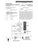
[0006]In FIG. 1, a charge amplifier configuration 10 is shown, where vn2 represents a noise power from signal processing electronics following the charge amplifier; such as a filter, buffer, analog-to-digital converter, and the like.
[0007]In order to make the noise contribution from the processing electronics negligible compared to the signal voltage, which is determined by V=Q/C, a charge-to-voltage conversion gain 1/C is preferably maximized. This can be achieved by minimizing the value of C. Assuming a noiseless charge amplifier, the signal-to-noise ratio is given by
Q / ( C v n 2 _ ) , ##EQU00001##
and the minimum detectable charge is given by
Q min ≈ C v n 2 _ . ##EQU00002##
On the other hand, a saturation voltage of the amplifier, which is equal to the supply voltage VDD in an ideal case, limits the measurable charge Q to a maximum value QMAX=VDDC. An assumption is made that the virtual ground input of the amplifier is at 0V.
[0008]The result is that a dynamic range QMAX/QMIN of the configuration shown in FIG. 1 is independent of C and given by
V DD / v n 2 _ . ##EQU00003##
Even if the dynamic range can be improved by filtering performed in the signal processing stage, the result is limited by technology and system constraints to typically no more than a few hundred, such as 100-300.
[0009]Therefore, it would be advantageous if the dynamic range in charge amplifier configurations could be increased to well above a few hundred once technology and system constraints, such as signal processing and associated noise, are taken into consideration.
SUMMARY OF THE INVENTION
[0010]The present invention relates to a charge amplifier for use in radiation sensing, which includes an amplifier including an input, at least one switch including an input, wherein the switch selectively couples the input of the switch to one of at least two voltages, and at least one capacitor electrically coupled in series between the input of the amplifier and the input of the switch, the capacitor is electrically coupled to the input of the operational amplifier without a switch coupled therebetween.
[0011]The amplifier may include an output and an operational amplifier, the input of the amplifier is operatively coupled to an anode of the operational amplifier, and the output of the amplifier is operatively coupled to a cathode of the operational amplifier. The charge amplifier may include a second capacitor electrically coupled in parallel with the amplifier. The charge amplifier may include a comparator including a first input, a second input, and an output, wherein the first input is operatively coupled to the output of the amplifier and the second input is operatively coupled to a threshold voltage, and a logic device operatively coupled to the output of the comparator. The logic device may control the switch in response to the output of the comparator.
[0012]The voltages may include a first voltage less than a second voltage, wherein the logic device controls the at least one switch to couple the input of the switch to the second voltage in response to the output of the amplifier being greater than the threshold voltage. The logic device may control the switch to couple the input of the switch to the first voltage in response to the output of the amplifier being less than the threshold voltage. The charge amplifier may be implemented using at least one of an Application Specific Integrated Circuit (ASIC), a microprocessor, a microcontroller, a programmable logic device, and/or a gate array
[0013]The present invention further relates to a method of measuring charge in radiation sensing, which includes selectively diverting charge from an input of an amplifier to an input of at least one capacitor by selectively coupling an output of the at least one capacitor to one of at least two voltages, wherein the input of the capacitor is operatively coupled to the input of the amplifier without a switch coupled therebetween, and calculating a total charge based on a sum of the amplified charge and the diverted charge.
[0014]The method may include comparing voltage at the output of the amplifier to a threshold voltage, and controlling the selective diversion of charge from the input of the amplifier to the input of the capacitor based on the comparison. The method may include controlling the selective diversion of charge from the input of the amplifier to the input of the capacitor by operatively coupling an output of the capacitor to the second voltage in response to the output of the amplifier being greater than the threshold voltage. The method may include controlling the selective diversion of charge from the input of the amplifier to the input of the at least one capacitor by operatively coupling an output of the capacitor to the first voltage in response to the output of the amplifier being less than the threshold voltage. The method may include implementing the charge amplifier using at least one of an Application Specific Integrated Circuit (ASIC), a microprocessor, a microcontroller, a programmable logic device, and/or a gate array.
[0015]The present invention still further relates to a computer-readable medium including instructions, wherein execution of the instructions by at least one computing device controls measurement of charge in radiation sensing by selectively diverting charge from an input of an amplifier to an input of at least one capacitor by selectively coupling an output of the capacitor to one of at least two voltages, wherein the input of the capacitor is operatively coupled to the input of the amplifier without a switch coupled therebetween, and calculating a total charge based on a sum of the amplified charge and the diverted charge.
[0016]Execution of the instructions by at least one computing device may control measurement of charge in radiation sensing by coupling a second capacitor electrically in parallel with the amplifier. Execution of the instructions by at least one computing device may control measurement of charge in radiation sensing by comparing voltage at the output of the amplifier to a threshold voltage, and controlling the selective diversion of charge from the input of the amplifier to the input of the capacitor based on the comparison. Execution of the instructions may control measurement of charge in radiation sensing by controlling the selective diversion of charge from the input of the amplifier to the input of the at least one capacitor by operatively coupling an output of the at least one capacitor to the second voltage in response to the output of the amplifier being greater than the threshold voltage. Execution of the instructions may control measurement of charge in radiation sensing by controlling the selective diversion of charge from the input of the amplifier to the input of the capacitor by operatively coupling an output of the capacitor to the first voltage in response to the output of the amplifier being less than the threshold voltage.
[0017]Other objects and features of the present invention will become apparent from the following detailed description considered in conjunction with the accompanying drawings. It is to be understood, however, that the drawings are designed as an illustration only and not as a definition of the limits of the invention.
BRIEF DESCRIPTION OF THE DRAWINGS
[0018]FIG. 1 is a block diagram of a conventional charge amplifier configuration.
[0019]FIG. 2 is a block diagram of a charge amplifier in a multiple-gain configuration.
[0020]FIG. 3 is a block diagram of a charge amplifier in a charge-pump configuration.
[0021]FIG. 4 is a block diagram of a charge amplifier in a capacitive charge-pump configuration.
[0022]FIG. 5 is a block diagram of a charge amplifier configuration in accordance with a first embodiment of the present invention.
[0023]FIG. 6 is a block diagram of a charge amplifier configuration in accordance with a second embodiment of the present invention.
[0024]FIG. 7 is a flow chart of a method for determining charge using the charge amplifier configuration shown in FIG. 5.
DETAILED DESCRIPTION OF THE EMBODIMENTS
[0025]To increase dynamic range in charge amplifiers, three methods are proposed: a multiple-gain method, a current charge-pump method, and a capacitive charge-pump method.
Multiple-Gain Method
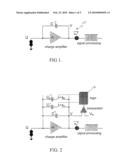
[0026]This method includes progressively reducing the gain by adding in parallel to C one or more capacitors Cj through switches sj, as shown in FIG. 2 and described in greater detail in V. Bonvicini, G. Orzan, G. Zampa, "CASIS10: A Prototype VLSI Front-End ASIC with Ultra-Large Dynamic Range and Integrated ADC for Silicon Calorimetry in Space Experiments," Nucl. Instrum. Methods, A 572, pp. 340-344, 2007, which is incorporated herein by reference. If the output voltage V exceeds a threshold Vth, a logic circuit 12 enables a first capacitor C1 to reduce the gain from 1/C to 1/(C+C1). If after enabling C1, V does not fall below the threshold, the logic circuit 12 enables connects a second capacitor C2, reducing the gain to 1/(C+C1+C2). This sequence continues for an arbitrary number of capacitors until V falls below the threshold. The closed switches preferably define the charge-to-voltage conversion gain to be applied to the resulting voltage V. The values of the capacitors Cj are preferably chosen to cover the dynamic range of interest. When the switch sj is open, the terminal of the capacitor Cj can be connected either to the input or to ground, the latter is preferred to avoid charge injection from switches connected to the input.
[0027]The disadvantage of this method is that the reduction in gain limits the signal-to-noise ratio to that achievable with the configuration shown in FIG. 1. Accordingly, with one capacitor, the maximum signal-to-noise ratio is given by
V DD C / ( C v n 2 _ ) = V DD v n 2 _ ##EQU00004##
Likewise, with N capacitors, the maximum dynamic range is identically given by
V DD NC / ( NC v n 2 _ ) = V DD v n 2 _ . ##EQU00005##
Current Charge-Pump Method
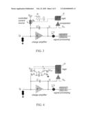
[0028]This method includes subtracting charge by enabling a controlled current source of value ip for fixed time intervals Δtj, as shown in FIG. 3 and described in greater detail in E. Kraft, P. Fisher, M. Karagounis, M. Koch, H. Krueger, I. Peric, N. Wermes, C. Herrmann, A. Nascetti, M. Overdick, and W. Ruetten, "Counting and Integrating Readout for Direct conversion X-ray Imaging: Concept, Realization and First Prototype Measurements," IEEE Trans. Nucl. Sci., vol. 54, pp. 383-390, 2007, which is incorporated herein by reference. If the output voltage V exceeds a threshold Vth, the logic circuit 14 generates a first control pulse having a duration Δt1, which subtracts a fixed charge qp1=ipΔt1. If after the first control pulse V does not fall below the threshold, the logic circuit 14 generates a second control pulse of duration Δt2, which subtracts another fixed charge qp2=ipΔt2. This sequence continues until V falls below the threshold. The number and duration of pulses defines the charge to be added to that measured from the resulting voltage V.
[0029]The disadvantage of this method is the length of time required for the entire integration to be performed, which is derived from the requirement concerning the accuracy of Δt. If qp=ipΔt is the subtracted charge and σt is the time jitter on Δt, the noise associated with the charge subtraction is given by σq=σtip=σtqp/Δt. The noise can then be reduced by increasing Δt, but the duration of the integration increases accordingly.
Capacitive Charge-Pump Method
[0030]This method includes subtracting amounts of charge by charging and discharging a capacitor Cp, as shown in FIG. 4 and described in further detail in G. Mazza, R. Cirio, M. Donetti, A. La Rose, A. Luparia, F. Marchetto, and C. Peroni, "A 64-Channel Wide Dynamic Range Charge Measurement ASIC for Strip and Pixel Ionization Detectors," IEEE Trans. Nucl. Sci, vol. 52, pp. 847-853, 2005, which is incorporated herein by reference. The reference voltage Vref is assumed to be equal to the amplifier input voltage. If the output voltage V exceeds a threshold Vth, a logic circuit 16 generates a first cycle of control pulses that opens switches S1 and S2 and closes switches S3 and S4, which subtracts a fixed charge q=VDD/Cp. If after the first cycle of control pulses, V does not fall below the threshold, the logic circuit 16 generates a second cycle of control pulses, which subtracts another fixed charge q. This sequence continues for an arbitrary number of control pulses until V falls below the threshold. The number of control cycles defines the charge to be added to that measured from the resulting voltage V.
[0031]The disadvantage of this method is that it requires a switch connected to the input node of the charge amplifier. As a consequence, parasitic charge is injected during the switching activity.
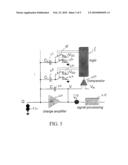
[0032]FIG. 5 shows a preferred embodiment of a charge amplifier formed in accordance with the present invention. The charge amplifier includes an operational amplifier 20, which is responsive to an applied charge source 22 and outputs a voltage to a signal processing circuit 24. A capacitor 26 is electronically coupled in parallel with the operational amplifier 20, that is, the capacitor 26 is connected across the anode and cathode of the operational amplifier 20. Another capacitor 28 is electronically coupled in series between the anode of the operational amplifier 20 and a bank of switches S1b 32 and S1a 30 with common input. Yet another capacitor 34 is shown connected (similarly to capacitor 28) electrically in series between the anode of operational amplifier 20 and a bank of switches S2a 36 and S2b 38. The logic circuit 18 preferably controls each of the switches S1a 30, S1b 32, S2a 36, and S2b 38. One input of a comparator 40 is preferably connected to the cathode of the operational amplifier 20, and a remaining input of comparator 40 is connected to a threshold voltage Vth. The output of comparator 40 is then provided to the logic circuit 18.
[0033]The method in accordance with the present invention subtracts amounts of charge by using a number of additional capacitors Cj controlled through switches Sja and Sjb, as shown in FIG. 5. If the output voltage V exceeds a threshold voltage Vth, the logic circuit 18, by opening S1a and closing S1b, routes the terminal of a first capacitor C1 from a first fixed voltage V1 (which is preferably ground, as shown in FIG. 5) to a higher fixed voltage V2 (preferably the supply VDD shown in FIG. 5), thereby subtracting a charge C1(V2-V1) (C1VDD in the case of FIG. 5). If after the first subtraction V does not fall below the threshold, the logic circuit 18 preferably performs a second subtraction C2(V2-V1) through a second capacitor C2. This sequence continues until V does fall below the threshold. The number of subtractions, along with the associated Cj, defines the charge to be added to that measured from the resulting voltage V. The values of the capacitors Cj are chosen to cover the dynamic range of interest.
[0034]The configuration shown in FIG. 5 is intended for measuring positive charges. A configuration for measuring negative charges can also be realized by inverting VDD and ground at each of the switches SJa and SJb in FIG. 5). For example, switch S1a 30 is connected to the higher fixed voltage V2, which is preferably VDD, and switch S1b 32 is connected to the lower fixed voltage V1, which is preferably ground, as shown in FIG. 6.
[0035]FIG. 7 shows a flow chart of the method for use in accordance with a charge amplifier configuration shown in FIG. 5. Each of these switches, as designated by J=1 to N, where N is the total number of Sa switches and total number of Sb switches, is initiated by closing the SJa switches for J=1 to N and opening the SJb switches for J=1 to N in step 42. J, an index variable, is then initialized to 0 in step 44 and the charge to be determined is inputted in step 46. If V is greater than Vth in step 48, then J is incremented by 1 instead of 50. VSa switch corresponding to the current value of J is then opened, and the VSb switch corresponding to the current value of J is closed in step 52 and the voltage V is then checked against the Vth in step 48.
[0036]If the voltage V is not greater than Vth in step 48, the measured charge is applied to the signal processing circuit in step 54. The subtracted charged is then calculated in step 56 using the following equation:
i = 1 j C i ( V 2 - V 1 ) ##EQU00006##
[0037]The subtracted charge calculated in step 56 is then added to the measured charge determined in step 54 to determine the total charge in step 58.
[0038]As an example, if the total charge were Q=1.1 pC (picocoulombs), Cj=0.1pF, and V2-V1=2.5V, then four (4) subtractions would be required, each being of 0.25 coulombs, yielding a subtracted charge of 1.0 picocoulombs and a measured charge of 0.1 picocoulombs.
[0039]Thus, the method of the present invention advantageously increases the dynamic range of a charge amplifier without requiring accurate timing signals or switches connected to the input of the charge amplifier. The present invention also provides the advantage of a signal-to-noise ratio that is not limited to that achievable using the configuration shown in FIG. 1. In the case of FIG. 5 and assuming identical Cj, for a given charge Q, the resulting voltage is given by V=Q/C-NVDD where N is the number of subtractions. The maximum signal-to-noise ration or dynamic range is then effectively given by
[ V DD + NV DD ] C / ( C v n 2 _ ) = V DD ( N + 1 ) v n 2 _ ##EQU00007##
which increases with N.Although illustrative embodiments of the present invention have been described herein with reference to the accompanying drawing, it is to be understood that the invention is not limited to those precise embodiments, and that various other changes and modifications may be effected therein by one skilled in the art without departing from the scope or spirit of the invention.
Claims:
1. A charge amplifier adapted to be used in radiation sensing
comprising:an amplifier including an input;at least one switch including
an input, the at least one switch selectively coupling the input of the
at least one switch to one of at least two voltages; andat least one
capacitor electrically coupled in series between the input of the
amplifier and the input of the switch, the at least one capacitor being
electrically coupled to the input of the amplifier without a switch
coupled therebetween.
2. The charge amplifier defined by claim 1, wherein the amplifier includes an output and an operational amplifier, the input of the amplifier being operatively coupled to an anode of the operational amplifier, the output of the amplifier being operatively coupled to a cathode of the operational amplifier.
3. The charge amplifier defined by claim 1, further comprising a second capacitor electrically coupled in parallel with the amplifier.
4. The charge amplifier defined by claim 1, wherein the amplifier includes an output, the charge amplifier further comprising:a comparator including a first input, a second input, and an output, the first input operatively coupled to the output of the amplifier, the second input operatively coupled to a threshold voltage; anda logic device operatively coupled to the output of the comparator, the logic device controlling the at least one switch in response to the output of the comparator.
5. The charge amplifier defined by claim 4, wherein the at least two voltages include a first voltage and a second voltage, the first voltage being less than the second voltage, the logic device controlling the at least one switch to couple the input of the at least one switch to the second voltage in response to the output of the amplifier being greater than the threshold voltage.
6. The charge amplifier defined by claim 4, wherein the at least two voltages include a first voltage and a second voltage, the first voltage being less than the second voltage, the logic device controlling the at least one switch to couple the input of the at least one switch to the first voltage in response to the output of the amplifier being less than the threshold voltage.
7. The charge amplifier defined by claim 1, wherein the charge amplifier is implemented using at least one of an Application Specific Integrated Circuit (ASIC), a microprocessor, a microcontroller, a programmable logic device, and a gate array.
8. A method of measuring charge in radiation sensing comprising:selectively diverting charge from an input of an amplifier to an input of at least one capacitor by selectively coupling an output of the at least one capacitor to one of at least two voltages, the input of the at least one capacitor being operatively coupled to the input of the amplifier without a switch coupled therebetween; andcalculating a total charge based on a sum of the amplified charge and the diverted charge.
9. The method of amplifying charge in radiation sensing defined by claim 8, wherein the amplifier includes an output and an operational amplifier, the input of the amplifier being operatively coupled to an anode of the operational amplifier, the output of the amplifier being operatively coupled to a cathode of the operational amplifier.
10. The method of amplifying charge in radiation sensing defined by claim 8, further comprising coupling a second capacitor electrically in parallel with the amplifier.
11. The method of amplifying charge in radiation sensing defined by claim 8, wherein the amplifier includes an output, the method further comprising:comparing voltage at the output of the amplifier to a threshold voltage; andcontrolling the selective diversion of charge from the input of the amplifier to the input of the at least one capacitor based on the comparison.
12. The method of amplifying charge in radiation sensing defined by claim 11, wherein the at least two voltages include a first voltage and a second voltage, the first voltage being less than the second voltage, the method further comprising controlling the selective diversion of charge from the input of the amplifier to the input of the at least one capacitor by operatively coupling an output of the at least one capacitor to the second voltage in response to the output of the amplifier being greater than the threshold voltage.
13. The method of amplifying charge in radiation sensing defined by claim 11, wherein the at least two voltages include a first voltage and a second voltage, the first voltage being less than the second voltage, the method further comprising controlling the selective diversion of charge from the input of the amplifier to the input of the at least one capacitor by operatively coupling an output of the at least one capacitor to the first voltage in response to the output of the amplifier being less than the threshold voltage.
14. The method of amplifying charge in radiation sensing defined by claim 8, further comprising implementing the charge amplifier using at least one of an Application Specific Integrated Circuit (ASIC), a microprocessor, a microcontroller, a programmable logic device, and a gate array.
15. A computer-readable medium comprising instructions, wherein execution of the instructions by at least one computing device controls measurement of charge in radiation sensing by:selectively diverting charge from an input of an amplifier to an input of at least one capacitor by selectively coupling an output of the at least one capacitor to one of at least two voltages, the input of the at least one capacitor being operatively coupled to the input of the amplifier without a switch coupled therebetween; andcalculating a total charge based on a sum of the amplified charge and the diverted charge.
16. The computer-readable medium defined by claim 15, wherein the amplifier includes an output and an operational amplifier, the input of the amplifier being operatively coupled to an anode of the operational amplifier, the output of the amplifier being operatively coupled to a cathode of the operational amplifier.
17. The computer-readable medium defined by claim 15, wherein execution of the instructions by at least one computing device controls amplification of charge in radiation sensing by coupling a second capacitor electrically in parallel with the amplifier.
18. The computer-readable medium defined by claim 15, wherein the amplifier includes an output, wherein execution of the instructions by at least one computing device controls amplification of charge in radiation sensing by:comparing voltage at the output of the amplifier to a threshold voltage; andcontrolling the selective diversion of charge from the input of the amplifier to the input of the at least one capacitor based on the comparison.
19. The computer-readable medium comprising instructions defined by claim 15, wherein the at least two voltages include a first voltage and a second voltage, the first voltage being less than the second voltage, wherein execution of the instructions by at least one computing device controls amplification of charge in radiation sensing by, controlling the selective diversion of charge from the input of the amplifier to the input of the at least one capacitor by operatively coupling an output of the at least one capacitor to the second voltage in response to the output of the amplifier being greater than the threshold voltage.
20. The computer-readable medium comprising instructions defined by claim 15, wherein the at least two voltages include a first voltage and a second voltage, the first voltage being less than the second voltage, wherein execution of the instructions by at least one computing device controls amplification of charge in radiation sensing by, controlling the selective diversion of charge from the input of the amplifier to the input of the at least one capacitor by operatively coupling an output of the at least one capacitor to the first voltage in response to the output of the amplifier being less than the threshold voltage.
Description:
BACKGROUND OF THE INVENTION
[0002]1. Field of the Invention
[0003]The present invention relates to charge amplifiers for use in radiation sensors, and more particularly to such charge amplifiers that exhibit an increased dynamic range.
[0004]2. Description of the Prior Art
[0005]In radiation sensors, ionizing radiation generates free charges in an amount Q that is proportional to the energy of the ionizing radiation. Charge is typically quantified by using a low-noise charge amplifier, which performs an integration through a feedback capacitor C, thus converting the charge Q into a voltage V=Q/C.
[0006]In FIG. 1, a charge amplifier configuration 10 is shown, where vn2 represents a noise power from signal processing electronics following the charge amplifier; such as a filter, buffer, analog-to-digital converter, and the like.
[0007]In order to make the noise contribution from the processing electronics negligible compared to the signal voltage, which is determined by V=Q/C, a charge-to-voltage conversion gain 1/C is preferably maximized. This can be achieved by minimizing the value of C. Assuming a noiseless charge amplifier, the signal-to-noise ratio is given by
Q / ( C v n 2 _ ) , ##EQU00001##
and the minimum detectable charge is given by
Q min ≈ C v n 2 _ . ##EQU00002##
On the other hand, a saturation voltage of the amplifier, which is equal to the supply voltage VDD in an ideal case, limits the measurable charge Q to a maximum value QMAX=VDDC. An assumption is made that the virtual ground input of the amplifier is at 0V.
[0008]The result is that a dynamic range QMAX/QMIN of the configuration shown in FIG. 1 is independent of C and given by
V DD / v n 2 _ . ##EQU00003##
Even if the dynamic range can be improved by filtering performed in the signal processing stage, the result is limited by technology and system constraints to typically no more than a few hundred, such as 100-300.
[0009]Therefore, it would be advantageous if the dynamic range in charge amplifier configurations could be increased to well above a few hundred once technology and system constraints, such as signal processing and associated noise, are taken into consideration.
SUMMARY OF THE INVENTION
[0010]The present invention relates to a charge amplifier for use in radiation sensing, which includes an amplifier including an input, at least one switch including an input, wherein the switch selectively couples the input of the switch to one of at least two voltages, and at least one capacitor electrically coupled in series between the input of the amplifier and the input of the switch, the capacitor is electrically coupled to the input of the operational amplifier without a switch coupled therebetween.
[0011]The amplifier may include an output and an operational amplifier, the input of the amplifier is operatively coupled to an anode of the operational amplifier, and the output of the amplifier is operatively coupled to a cathode of the operational amplifier. The charge amplifier may include a second capacitor electrically coupled in parallel with the amplifier. The charge amplifier may include a comparator including a first input, a second input, and an output, wherein the first input is operatively coupled to the output of the amplifier and the second input is operatively coupled to a threshold voltage, and a logic device operatively coupled to the output of the comparator. The logic device may control the switch in response to the output of the comparator.
[0012]The voltages may include a first voltage less than a second voltage, wherein the logic device controls the at least one switch to couple the input of the switch to the second voltage in response to the output of the amplifier being greater than the threshold voltage. The logic device may control the switch to couple the input of the switch to the first voltage in response to the output of the amplifier being less than the threshold voltage. The charge amplifier may be implemented using at least one of an Application Specific Integrated Circuit (ASIC), a microprocessor, a microcontroller, a programmable logic device, and/or a gate array
[0013]The present invention further relates to a method of measuring charge in radiation sensing, which includes selectively diverting charge from an input of an amplifier to an input of at least one capacitor by selectively coupling an output of the at least one capacitor to one of at least two voltages, wherein the input of the capacitor is operatively coupled to the input of the amplifier without a switch coupled therebetween, and calculating a total charge based on a sum of the amplified charge and the diverted charge.
[0014]The method may include comparing voltage at the output of the amplifier to a threshold voltage, and controlling the selective diversion of charge from the input of the amplifier to the input of the capacitor based on the comparison. The method may include controlling the selective diversion of charge from the input of the amplifier to the input of the capacitor by operatively coupling an output of the capacitor to the second voltage in response to the output of the amplifier being greater than the threshold voltage. The method may include controlling the selective diversion of charge from the input of the amplifier to the input of the at least one capacitor by operatively coupling an output of the capacitor to the first voltage in response to the output of the amplifier being less than the threshold voltage. The method may include implementing the charge amplifier using at least one of an Application Specific Integrated Circuit (ASIC), a microprocessor, a microcontroller, a programmable logic device, and/or a gate array.
[0015]The present invention still further relates to a computer-readable medium including instructions, wherein execution of the instructions by at least one computing device controls measurement of charge in radiation sensing by selectively diverting charge from an input of an amplifier to an input of at least one capacitor by selectively coupling an output of the capacitor to one of at least two voltages, wherein the input of the capacitor is operatively coupled to the input of the amplifier without a switch coupled therebetween, and calculating a total charge based on a sum of the amplified charge and the diverted charge.
[0016]Execution of the instructions by at least one computing device may control measurement of charge in radiation sensing by coupling a second capacitor electrically in parallel with the amplifier. Execution of the instructions by at least one computing device may control measurement of charge in radiation sensing by comparing voltage at the output of the amplifier to a threshold voltage, and controlling the selective diversion of charge from the input of the amplifier to the input of the capacitor based on the comparison. Execution of the instructions may control measurement of charge in radiation sensing by controlling the selective diversion of charge from the input of the amplifier to the input of the at least one capacitor by operatively coupling an output of the at least one capacitor to the second voltage in response to the output of the amplifier being greater than the threshold voltage. Execution of the instructions may control measurement of charge in radiation sensing by controlling the selective diversion of charge from the input of the amplifier to the input of the capacitor by operatively coupling an output of the capacitor to the first voltage in response to the output of the amplifier being less than the threshold voltage.
[0017]Other objects and features of the present invention will become apparent from the following detailed description considered in conjunction with the accompanying drawings. It is to be understood, however, that the drawings are designed as an illustration only and not as a definition of the limits of the invention.
BRIEF DESCRIPTION OF THE DRAWINGS
[0018]FIG. 1 is a block diagram of a conventional charge amplifier configuration.
[0019]FIG. 2 is a block diagram of a charge amplifier in a multiple-gain configuration.
[0020]FIG. 3 is a block diagram of a charge amplifier in a charge-pump configuration.
[0021]FIG. 4 is a block diagram of a charge amplifier in a capacitive charge-pump configuration.
[0022]FIG. 5 is a block diagram of a charge amplifier configuration in accordance with a first embodiment of the present invention.
[0023]FIG. 6 is a block diagram of a charge amplifier configuration in accordance with a second embodiment of the present invention.
[0024]FIG. 7 is a flow chart of a method for determining charge using the charge amplifier configuration shown in FIG. 5.
DETAILED DESCRIPTION OF THE EMBODIMENTS
[0025]To increase dynamic range in charge amplifiers, three methods are proposed: a multiple-gain method, a current charge-pump method, and a capacitive charge-pump method.
Multiple-Gain Method
[0026]This method includes progressively reducing the gain by adding in parallel to C one or more capacitors Cj through switches sj, as shown in FIG. 2 and described in greater detail in V. Bonvicini, G. Orzan, G. Zampa, "CASIS10: A Prototype VLSI Front-End ASIC with Ultra-Large Dynamic Range and Integrated ADC for Silicon Calorimetry in Space Experiments," Nucl. Instrum. Methods, A 572, pp. 340-344, 2007, which is incorporated herein by reference. If the output voltage V exceeds a threshold Vth, a logic circuit 12 enables a first capacitor C1 to reduce the gain from 1/C to 1/(C+C1). If after enabling C1, V does not fall below the threshold, the logic circuit 12 enables connects a second capacitor C2, reducing the gain to 1/(C+C1+C2). This sequence continues for an arbitrary number of capacitors until V falls below the threshold. The closed switches preferably define the charge-to-voltage conversion gain to be applied to the resulting voltage V. The values of the capacitors Cj are preferably chosen to cover the dynamic range of interest. When the switch sj is open, the terminal of the capacitor Cj can be connected either to the input or to ground, the latter is preferred to avoid charge injection from switches connected to the input.
[0027]The disadvantage of this method is that the reduction in gain limits the signal-to-noise ratio to that achievable with the configuration shown in FIG. 1. Accordingly, with one capacitor, the maximum signal-to-noise ratio is given by
V DD C / ( C v n 2 _ ) = V DD v n 2 _ ##EQU00004##
Likewise, with N capacitors, the maximum dynamic range is identically given by
V DD NC / ( NC v n 2 _ ) = V DD v n 2 _ . ##EQU00005##
Current Charge-Pump Method
[0028]This method includes subtracting charge by enabling a controlled current source of value ip for fixed time intervals Δtj, as shown in FIG. 3 and described in greater detail in E. Kraft, P. Fisher, M. Karagounis, M. Koch, H. Krueger, I. Peric, N. Wermes, C. Herrmann, A. Nascetti, M. Overdick, and W. Ruetten, "Counting and Integrating Readout for Direct conversion X-ray Imaging: Concept, Realization and First Prototype Measurements," IEEE Trans. Nucl. Sci., vol. 54, pp. 383-390, 2007, which is incorporated herein by reference. If the output voltage V exceeds a threshold Vth, the logic circuit 14 generates a first control pulse having a duration Δt1, which subtracts a fixed charge qp1=ipΔt1. If after the first control pulse V does not fall below the threshold, the logic circuit 14 generates a second control pulse of duration Δt2, which subtracts another fixed charge qp2=ipΔt2. This sequence continues until V falls below the threshold. The number and duration of pulses defines the charge to be added to that measured from the resulting voltage V.
[0029]The disadvantage of this method is the length of time required for the entire integration to be performed, which is derived from the requirement concerning the accuracy of Δt. If qp=ipΔt is the subtracted charge and σt is the time jitter on Δt, the noise associated with the charge subtraction is given by σq=σtip=σtqp/Δt. The noise can then be reduced by increasing Δt, but the duration of the integration increases accordingly.
Capacitive Charge-Pump Method
[0030]This method includes subtracting amounts of charge by charging and discharging a capacitor Cp, as shown in FIG. 4 and described in further detail in G. Mazza, R. Cirio, M. Donetti, A. La Rose, A. Luparia, F. Marchetto, and C. Peroni, "A 64-Channel Wide Dynamic Range Charge Measurement ASIC for Strip and Pixel Ionization Detectors," IEEE Trans. Nucl. Sci, vol. 52, pp. 847-853, 2005, which is incorporated herein by reference. The reference voltage Vref is assumed to be equal to the amplifier input voltage. If the output voltage V exceeds a threshold Vth, a logic circuit 16 generates a first cycle of control pulses that opens switches S1 and S2 and closes switches S3 and S4, which subtracts a fixed charge q=VDD/Cp. If after the first cycle of control pulses, V does not fall below the threshold, the logic circuit 16 generates a second cycle of control pulses, which subtracts another fixed charge q. This sequence continues for an arbitrary number of control pulses until V falls below the threshold. The number of control cycles defines the charge to be added to that measured from the resulting voltage V.
[0031]The disadvantage of this method is that it requires a switch connected to the input node of the charge amplifier. As a consequence, parasitic charge is injected during the switching activity.
[0032]FIG. 5 shows a preferred embodiment of a charge amplifier formed in accordance with the present invention. The charge amplifier includes an operational amplifier 20, which is responsive to an applied charge source 22 and outputs a voltage to a signal processing circuit 24. A capacitor 26 is electronically coupled in parallel with the operational amplifier 20, that is, the capacitor 26 is connected across the anode and cathode of the operational amplifier 20. Another capacitor 28 is electronically coupled in series between the anode of the operational amplifier 20 and a bank of switches S1b 32 and S1a 30 with common input. Yet another capacitor 34 is shown connected (similarly to capacitor 28) electrically in series between the anode of operational amplifier 20 and a bank of switches S2a 36 and S2b 38. The logic circuit 18 preferably controls each of the switches S1a 30, S1b 32, S2a 36, and S2b 38. One input of a comparator 40 is preferably connected to the cathode of the operational amplifier 20, and a remaining input of comparator 40 is connected to a threshold voltage Vth. The output of comparator 40 is then provided to the logic circuit 18.
[0033]The method in accordance with the present invention subtracts amounts of charge by using a number of additional capacitors Cj controlled through switches Sja and Sjb, as shown in FIG. 5. If the output voltage V exceeds a threshold voltage Vth, the logic circuit 18, by opening S1a and closing S1b, routes the terminal of a first capacitor C1 from a first fixed voltage V1 (which is preferably ground, as shown in FIG. 5) to a higher fixed voltage V2 (preferably the supply VDD shown in FIG. 5), thereby subtracting a charge C1(V2-V1) (C1VDD in the case of FIG. 5). If after the first subtraction V does not fall below the threshold, the logic circuit 18 preferably performs a second subtraction C2(V2-V1) through a second capacitor C2. This sequence continues until V does fall below the threshold. The number of subtractions, along with the associated Cj, defines the charge to be added to that measured from the resulting voltage V. The values of the capacitors Cj are chosen to cover the dynamic range of interest.
[0034]The configuration shown in FIG. 5 is intended for measuring positive charges. A configuration for measuring negative charges can also be realized by inverting VDD and ground at each of the switches SJa and SJb in FIG. 5). For example, switch S1a 30 is connected to the higher fixed voltage V2, which is preferably VDD, and switch S1b 32 is connected to the lower fixed voltage V1, which is preferably ground, as shown in FIG. 6.
[0035]FIG. 7 shows a flow chart of the method for use in accordance with a charge amplifier configuration shown in FIG. 5. Each of these switches, as designated by J=1 to N, where N is the total number of Sa switches and total number of Sb switches, is initiated by closing the SJa switches for J=1 to N and opening the SJb switches for J=1 to N in step 42. J, an index variable, is then initialized to 0 in step 44 and the charge to be determined is inputted in step 46. If V is greater than Vth in step 48, then J is incremented by 1 instead of 50. VSa switch corresponding to the current value of J is then opened, and the VSb switch corresponding to the current value of J is closed in step 52 and the voltage V is then checked against the Vth in step 48.
[0036]If the voltage V is not greater than Vth in step 48, the measured charge is applied to the signal processing circuit in step 54. The subtracted charged is then calculated in step 56 using the following equation:
i = 1 j C i ( V 2 - V 1 ) ##EQU00006##
[0037]The subtracted charge calculated in step 56 is then added to the measured charge determined in step 54 to determine the total charge in step 58.
[0038]As an example, if the total charge were Q=1.1 pC (picocoulombs), Cj=0.1pF, and V2-V1=2.5V, then four (4) subtractions would be required, each being of 0.25 coulombs, yielding a subtracted charge of 1.0 picocoulombs and a measured charge of 0.1 picocoulombs.
[0039]Thus, the method of the present invention advantageously increases the dynamic range of a charge amplifier without requiring accurate timing signals or switches connected to the input of the charge amplifier. The present invention also provides the advantage of a signal-to-noise ratio that is not limited to that achievable using the configuration shown in FIG. 1. In the case of FIG. 5 and assuming identical Cj, for a given charge Q, the resulting voltage is given by V=Q/C-NVDD where N is the number of subtractions. The maximum signal-to-noise ration or dynamic range is then effectively given by
[ V DD + NV DD ] C / ( C v n 2 _ ) = V DD ( N + 1 ) v n 2 _ ##EQU00007##
which increases with N.Although illustrative embodiments of the present invention have been described herein with reference to the accompanying drawing, it is to be understood that the invention is not limited to those precise embodiments, and that various other changes and modifications may be effected therein by one skilled in the art without departing from the scope or spirit of the invention.
User Contributions:
Comment about this patent or add new information about this topic:
Images included with this patent application:
 |  |
 |  |
 |  |
| New patent applications in this class: | |
| Date | Title |
|---|---|
| 2022-05-05 | Apparatus for testing electronic devices |
| 2019-05-16 | Input circuit for the fail-safe reading in of an analog input signal |
| 2016-07-07 | Method and system and computer program for measuring alternating-current system quantities |
| 2016-06-30 | Apparatus for testing electronic devices |
| 2016-06-23 | Method and system for determining the thermal power line rating |
| New patent applications from these inventors: | |
| Date | Title |
|---|---|
| 2015-11-05 | Method and apparatus for current-output peak detection |
| 2015-03-05 | Method and apparatus for sub-hysteresis discrimination |
| 2014-08-21 | Radiation detector device for rejecting and excluding incomplete charge collection events |
| 2014-08-07 | Array of virtual frisch-grid detectors with common cathode and reduced length of shielding electrodes |
| 2014-07-03 | Shaper design in cmos for high dynamic range |
| Top Inventors for class "Data processing: measuring, calibrating, or testing" | |
| Rank | Inventor's name |
|---|---|
| 1 | Lowell L. Wood, Jr. |
| 2 | Roderick A. Hyde |
| 3 | Shelten Gee Jao Yuen |
| 4 | James Park |
| 5 | Chih-Kuang Chang |