Patent application title: SINGLE-ENDED SENSE AMPLIFIER USING DYNAMIC REFERENCE VOLTAGE AND OPERATION METHOD THEREOF
Inventors:
Meng-Fan Chang (Taichung City, TW)
Meng-Fan Chang (Taichung City, TW)
Shu Meng Yang (Hualien County, TW)
Jiunn Way Miaw (Hsinchu City, TW)
Assignees:
INDUSTRIAL TECHNOLOGY RESEARCH INSTITUTE
IPC8 Class: AH03F345FI
USPC Class:
327563
Class name: Specific identifiable device, circuit, or system nonlinear amplifying circuit with differential amplifier
Publication date: 2010-02-18
Patent application number: 20100039173
al sense amplifier comprises a dynamic reference
voltage generation circuit and a differential sense amplifier circuit.
Input data with an input data line voltage is provided to the
differential sense amplifier circuit. The input data line voltage also
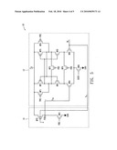
feeds back to the dynamic reference voltage generation circuit, which
then generates a dynamic reference voltage based on the input data line
voltage. The differential sense amplifier circuit is coupled to the
dynamic reference voltage generation circuit and receives the dynamic
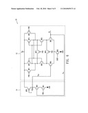
reference voltage for determining the input data. The dynamic reference
voltage increases and the input data line voltage decreases when reading
the input data of a logic state, e.g., logic "0."Claims:
1. A single-ended differential sense amplifier, comprising:a differential
sense amplifier circuit receiving input data from a data line; anda
dynamic reference voltage generation circuit tracking an input data line
voltage of the input data and being coupled to the differential sense
amplifier circuit, and generating a dynamic reference voltage based on
the input data line voltage to the differential sense amplifier circuit
for reading the input data.
2. The single-ended differential sense amplifier in accordance with claim 1, wherein the dynamic reference voltage increases and the input data line voltage decreases when reading the input data of a logic state.
3. The single-ended differential sense amplifier in accordance with claim 2, wherein the logic state is logic zero.
4. The single-ended differential sense amplifier in accordance with claim 1, wherein the dynamic reference voltage generation circuit comprises a PMOS transistor, a first NMOS transistor and a second NMOS transistor that collectively form a cascade down to ground.
5. The single-ended differential sense amplifier in accordance with claim 4, wherein the dynamic reference voltage is generated at a node between the PMOS transistor and the first NMOS transistor.
6. The single-ended differential sense amplifier in accordance with claim 4, wherein the input data line voltage is applied to the body of the PMOS transistor and the gate of the first NMOS transistor.
7. The single-ended differential sense amplifier in accordance with claim 1, wherein the dynamic reference voltage generation circuit comprises a PMOS transistor and a NMOS transistor that collectively form a cascade down to ground, and the input data line voltage is applied to the body of the PMOS transistor.
8. The single-ended differential sense amplifier in accordance with claim 1, wherein the dynamic reference voltage generation circuit comprises a PMOS transistor and a NMOS transistor that collectively form a cascade down to ground, and the input data line voltage is applied to the gate of the NMOS transistor.
9. The single-ended differential sense amplifier in accordance with claim 1, wherein the differential sense amplifier circuit comprises:two pre-charge transistors;a sensing transistor pair; anda cross-coupled latch coupled to the pre-charge transistors and the sensing transistor pair;wherein the two pre-charge transistors, the sensing pair transistors and the cross-coupled latch are symmetrical, and the sensing transistor pair is coupled to the dynamic reference voltage generation circuit to receive the dynamic reference voltage.
10. The single-ended differential sense amplifier in accordance with claim 9, wherein the differential sense amplifier circuit further comprises:equalizer transistors coupled between the sensing transistor pair and the cross-coupled latch; anda sensing enable switch coupled between the sensing transistor pair and ground.
11. An operation method for a single-ended differential sense amplifier, comprising the steps of:providing input data to the single-ended differential sense amplifier;generating a dynamic reference voltage based on an input data line voltage of the input data, wherein the input data line voltage decreases and the dynamic reference voltage increases when reading the input data of a logic state; andactivating the single-ended differential sense amplifier when the data line voltage is less than the dynamic reference voltage by a difference that is greater than a threshold value.
12. The operation method for a single-ended differential sense amplifier in accordance with claim 11, wherein the logic state is logic zero.
13. The operation method for a single-ended differential sense amplifier in accordance with claim 11, wherein the single-ended differential sense amplifier comprises a dynamic reference voltage generation circuit and a differential sense amplifier circuit, the dynamic reference voltage generation circuit receives the input data line voltage for generating the dynamic reference voltage, and the differential sense amplifier circuit compares the dynamic reference voltage and the input data line voltage to determine the logic state of the input data.Description:
BACKGROUND OF THE INVENTION
[0001](A) Field of the Invention
[0002]The present invention relates to a single-ended sense amplifier, and more particularly, to a single-ended sense amplifier using a dynamic reference voltage and the operation method thereof.
[0003](B) Description of the Related Art
[0004]In a conventional sense amplifier scheme, memory read operation is achieved by comparing input data with a reference voltage to determine the logic state of the input data. Hence, various types of sense amplifiers have been developed accordingly. The single-ended sense amplifier that is coupled to a single bit line is widely used in single-ended type memory designs, and can be attributed to two design styles. Many single-ended type memory designs employ an inverter as a sense amplifier. Such designs mainly use an inverter trip point as a reference voltage level. Consequently, the inverter trip point has to be carefully selected to decrease process-voltage-temperature (PVT) dependence. Reducing process-voltage-temperature (PVT) dependence, however, is not easy. Also, the inverter type sense amplifier is not suitable for large capacity memory designs due to slow bit line discharging time during read "0" operations, resulting in poor speed performance.
[0005]Another style of single-ended sense amplifier employs a differential sense amplifier with two inputs, of which one side is coupled to an input data line (bit line) and another side is coupled to a fixed reference voltage that comes from an additional reference voltage or an external voltage supply. This kind of sense amplifier design features a fast sensing speed, and is suitable for large capacity memories with proper reference voltage level adjustment and is robust enough for use in various PVT conditions. However, this sense amplifier occupies a greater area than that of the sense amplifier of an inverter type.
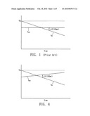
[0006]As shown in FIG. 1, the operation of a traditional single-ended differential sense amplifier refers to a fixed reference voltage VREF. The voltage of data line VDL decreases if the stored data is logic "0." When VDL falls below VREF and the voltage difference ΔV between VDL and VREF exceeds a threshold value, e.g., 100 mV, the stored data will be determined as "0" and the sense amplifier will be inverted or activated. However, VDL sometimes drops very slowly, and therefore may take a long time to reach the threshold value. With high-speed performance and large memory capacity requirements, the conventional fixed reference voltage level for sensing operation cannot meet the demand. Therefore, there is a demand to expedite operation efficiency.
SUMMARY OF THE INVENTION
[0007]The present invention is directed to providing a single-ended differential amplifier with high operation efficiency and the operation method thereof.
[0008]In accordance with the present invention, a single-ended differential sense amplifier comprises a dynamic reference voltage generation circuit and a differential sense amplifier circuit. Input data with an input data line voltage is provided to the differential sense amplifier circuit. The data line voltage also feeds back to the dynamic reference voltage generation circuit, which then generates a dynamic reference voltage based on the input data line voltage. The differential sense amplifier circuit is coupled to the dynamic reference voltage generation circuit and receives the dynamic reference voltage for determining the input data. The dynamic reference voltage increases and the input data line voltage decreases when reading the input data of a logic state, e.g., logic "0."
[0009]The operation for the single-ended differential sense amplifier may be described by the steps of: (1) providing input data with an input data line voltage to the single-ended differential sense amplifier; (2) generating a dynamic reference voltage based on the input data line voltage, wherein the dynamic reference voltage increases and the input data line voltage decreases when reading the input data of a logic state, e.g., logic zero; and (3) activating the single-ended differential sense amplifier when the input data line voltage is less than the dynamic reference voltage by a difference that is greater than a threshold value.
[0010]In order to make the aforementioned and other objectives, features, and advantages of the present invention more comprehensible, embodiments accompanied with figures are described in detail below.
BRIEF DESCRIPTION OF THE DRAWINGS
[0011]The objectives and advantages of the present invention will become apparent upon reading the following description and upon reference to the accompanying drawings in which:
[0012]FIG. 1 illustrates a known method for determining the logic state of the input data for a differential sense amplifier;
[0013]FIG. 2 illustrates a block diagram of the single-ended differential sense amplifier in accordance with the present invention;
[0014]FIG. 3 illustrates a single-ended differential sense amplifier in accordance with an embodiment of the present invention;
[0015]FIG. 4 illustrates the method for determining the logic state of the input data to a differential sense amplifier in accordance with the present invention; and
[0016]FIGS. 5 and 6 illustrate single-ended differential sense amplifiers in accordance with other embodiments of the present invention.
DETAILED DESCRIPTION OF THE INVENTION
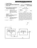
[0017]FIG. 2 illustrates a block diagram of a single-ended sense amplifier in accordance with the present invention. A single-ended sense amplifier 10 comprises a differential sense amplifier circuit 12 and a dynamic reference voltage generation circuit 14. The differential sense amplifier circuit 12 has two input ends, of which one end is coupled to a data line (bit line) so as to receive input data with a voltage VDL from the data line, and VDL also feeds back to the dynamic reference voltage generation circuit 14. The dynamic reference voltage generation circuit 14 generates a dynamic reference voltage VREF based on VDL, and VREF is transmitted to the other end of the differential sense amplifier circuit 12.
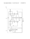
[0018]In an embodiment, as shown in FIG. 3, the single-ended sense amplifier 10 includes a differential sense amplifier circuit 12 and a feedback type dynamic reference voltage generation circuit 14. The dynamic reference voltage generation circuit 14 includes a PMOS transistor MP0, an NMOS transistor MN0 and an NMOS transistor MN1 that collectively form a cascade down to GND. The differential sense amplifier 12 includes pre-charge PMOS transistors MP1 and MP4, a cross-coupled latch consisting of MP2, MP3, MN2 and MN3, a sensing NMOS pair MN4 and MN5, equalizer PMOS transistors MP5 and MP6, and a sensing enable switch NMOS MN6. The cross-coupled latch consisting of MP2, MP3, MN2 and MN3 is coupled to the pre-charge transistors MP1 and MP4 and the sensing NMOS pair MN4 and MN5.
[0019]The dynamic reference voltage generation circuit 14 is an adjustable voltage divider which tracks data line (DL) node voltage level VDL applied to the gate of MN0 and the body of MP0 and generates feedback output voltage, i.e., reference voltage VREF, on the PZDL node. More specifically, the PZDL node is placed between MP0 and MN0, and is electrically coupled to the gate electrode of MN4. The differential sense amplifier circuit 12 is of symmetrical device size structure to minimize the mismatch influence on the sensing operation. During the sense amplifier evaluation period, control signals "PRE" and "SAEN" equal VDD and VSS (not shown in FIG. 2), respectively.
[0020]If the voltage level on DL node VDL equals VDD (i.e., stored data is logic "1"), MN0 will turn on and a stable and fixed reference voltage VREF will be generated. If the voltage level on DL node VDL decreases gradually from VDD (i.e., stored data is logic "0"), then the gate electrode of the NMOS transistor MN0 and the body electrode of the PMOS transistor MP0 will track VDL and reduce their current due to less Vgs and body effect, respectively, and consequently pull up feedback output voltage VREF on the PZDL node as illustrated in FIG. 4.
[0021]VREF is fixed in FIG. 1, whereas VREF in FIG. 4 increases over time. VDL drops gradually if the stored data is logic "0." Because VREF ramps up in FIG. 4, lines of VDD and VREF intersect earlier in comparison with that shown in FIG. 1. As such, a voltage difference ΔV between VDL and VREF exceeding a threshold value, e.g., 100 mV, will occur earlier. Accordingly, the sense amplifier with a dynamic reference voltage will invert or activate earlier in comparison with the sense amplifier with a fixed reference voltage, thereby increasing operation efficiency and the sensing margin for reading logic "0."
[0022]Alternatively, for the dynamic reference voltage generation circuit 14, VDL can be individually applied to either the body of the MP0 or the gate of MN0 as shown in FIG. 5 and FIG. 6, respectively. As such, the dynamic reference voltage generation circuit 14 can also provide the same function.
[0023]For the sense amplifier of the present invention, the sensing process can be accelerated with more sensing margin due to dynamic type reference voltage. Also, the sensing time is not sensitive to process variation because the reference voltage tracks the input data line in the memory array and symmetric structure of differential sense amplifier is employed in the present invention.
[0024]The above-described embodiments of the present invention are intended to be illustrative only. Numerous alternative embodiments may be devised by those skilled in the art without departing from the scope of the following claims.
Claims:
1. A single-ended differential sense amplifier, comprising:a differential
sense amplifier circuit receiving input data from a data line; anda
dynamic reference voltage generation circuit tracking an input data line
voltage of the input data and being coupled to the differential sense
amplifier circuit, and generating a dynamic reference voltage based on
the input data line voltage to the differential sense amplifier circuit
for reading the input data.
2. The single-ended differential sense amplifier in accordance with claim 1, wherein the dynamic reference voltage increases and the input data line voltage decreases when reading the input data of a logic state.
3. The single-ended differential sense amplifier in accordance with claim 2, wherein the logic state is logic zero.
4. The single-ended differential sense amplifier in accordance with claim 1, wherein the dynamic reference voltage generation circuit comprises a PMOS transistor, a first NMOS transistor and a second NMOS transistor that collectively form a cascade down to ground.
5. The single-ended differential sense amplifier in accordance with claim 4, wherein the dynamic reference voltage is generated at a node between the PMOS transistor and the first NMOS transistor.
6. The single-ended differential sense amplifier in accordance with claim 4, wherein the input data line voltage is applied to the body of the PMOS transistor and the gate of the first NMOS transistor.
7. The single-ended differential sense amplifier in accordance with claim 1, wherein the dynamic reference voltage generation circuit comprises a PMOS transistor and a NMOS transistor that collectively form a cascade down to ground, and the input data line voltage is applied to the body of the PMOS transistor.
8. The single-ended differential sense amplifier in accordance with claim 1, wherein the dynamic reference voltage generation circuit comprises a PMOS transistor and a NMOS transistor that collectively form a cascade down to ground, and the input data line voltage is applied to the gate of the NMOS transistor.
9. The single-ended differential sense amplifier in accordance with claim 1, wherein the differential sense amplifier circuit comprises:two pre-charge transistors;a sensing transistor pair; anda cross-coupled latch coupled to the pre-charge transistors and the sensing transistor pair;wherein the two pre-charge transistors, the sensing pair transistors and the cross-coupled latch are symmetrical, and the sensing transistor pair is coupled to the dynamic reference voltage generation circuit to receive the dynamic reference voltage.
10. The single-ended differential sense amplifier in accordance with claim 9, wherein the differential sense amplifier circuit further comprises:equalizer transistors coupled between the sensing transistor pair and the cross-coupled latch; anda sensing enable switch coupled between the sensing transistor pair and ground.
11. An operation method for a single-ended differential sense amplifier, comprising the steps of:providing input data to the single-ended differential sense amplifier;generating a dynamic reference voltage based on an input data line voltage of the input data, wherein the input data line voltage decreases and the dynamic reference voltage increases when reading the input data of a logic state; andactivating the single-ended differential sense amplifier when the data line voltage is less than the dynamic reference voltage by a difference that is greater than a threshold value.
12. The operation method for a single-ended differential sense amplifier in accordance with claim 11, wherein the logic state is logic zero.
13. The operation method for a single-ended differential sense amplifier in accordance with claim 11, wherein the single-ended differential sense amplifier comprises a dynamic reference voltage generation circuit and a differential sense amplifier circuit, the dynamic reference voltage generation circuit receives the input data line voltage for generating the dynamic reference voltage, and the differential sense amplifier circuit compares the dynamic reference voltage and the input data line voltage to determine the logic state of the input data.
Description:
BACKGROUND OF THE INVENTION
[0001](A) Field of the Invention
[0002]The present invention relates to a single-ended sense amplifier, and more particularly, to a single-ended sense amplifier using a dynamic reference voltage and the operation method thereof.
[0003](B) Description of the Related Art
[0004]In a conventional sense amplifier scheme, memory read operation is achieved by comparing input data with a reference voltage to determine the logic state of the input data. Hence, various types of sense amplifiers have been developed accordingly. The single-ended sense amplifier that is coupled to a single bit line is widely used in single-ended type memory designs, and can be attributed to two design styles. Many single-ended type memory designs employ an inverter as a sense amplifier. Such designs mainly use an inverter trip point as a reference voltage level. Consequently, the inverter trip point has to be carefully selected to decrease process-voltage-temperature (PVT) dependence. Reducing process-voltage-temperature (PVT) dependence, however, is not easy. Also, the inverter type sense amplifier is not suitable for large capacity memory designs due to slow bit line discharging time during read "0" operations, resulting in poor speed performance.
[0005]Another style of single-ended sense amplifier employs a differential sense amplifier with two inputs, of which one side is coupled to an input data line (bit line) and another side is coupled to a fixed reference voltage that comes from an additional reference voltage or an external voltage supply. This kind of sense amplifier design features a fast sensing speed, and is suitable for large capacity memories with proper reference voltage level adjustment and is robust enough for use in various PVT conditions. However, this sense amplifier occupies a greater area than that of the sense amplifier of an inverter type.
[0006]As shown in FIG. 1, the operation of a traditional single-ended differential sense amplifier refers to a fixed reference voltage VREF. The voltage of data line VDL decreases if the stored data is logic "0." When VDL falls below VREF and the voltage difference ΔV between VDL and VREF exceeds a threshold value, e.g., 100 mV, the stored data will be determined as "0" and the sense amplifier will be inverted or activated. However, VDL sometimes drops very slowly, and therefore may take a long time to reach the threshold value. With high-speed performance and large memory capacity requirements, the conventional fixed reference voltage level for sensing operation cannot meet the demand. Therefore, there is a demand to expedite operation efficiency.
SUMMARY OF THE INVENTION
[0007]The present invention is directed to providing a single-ended differential amplifier with high operation efficiency and the operation method thereof.
[0008]In accordance with the present invention, a single-ended differential sense amplifier comprises a dynamic reference voltage generation circuit and a differential sense amplifier circuit. Input data with an input data line voltage is provided to the differential sense amplifier circuit. The data line voltage also feeds back to the dynamic reference voltage generation circuit, which then generates a dynamic reference voltage based on the input data line voltage. The differential sense amplifier circuit is coupled to the dynamic reference voltage generation circuit and receives the dynamic reference voltage for determining the input data. The dynamic reference voltage increases and the input data line voltage decreases when reading the input data of a logic state, e.g., logic "0."
[0009]The operation for the single-ended differential sense amplifier may be described by the steps of: (1) providing input data with an input data line voltage to the single-ended differential sense amplifier; (2) generating a dynamic reference voltage based on the input data line voltage, wherein the dynamic reference voltage increases and the input data line voltage decreases when reading the input data of a logic state, e.g., logic zero; and (3) activating the single-ended differential sense amplifier when the input data line voltage is less than the dynamic reference voltage by a difference that is greater than a threshold value.
[0010]In order to make the aforementioned and other objectives, features, and advantages of the present invention more comprehensible, embodiments accompanied with figures are described in detail below.
BRIEF DESCRIPTION OF THE DRAWINGS
[0011]The objectives and advantages of the present invention will become apparent upon reading the following description and upon reference to the accompanying drawings in which:
[0012]FIG. 1 illustrates a known method for determining the logic state of the input data for a differential sense amplifier;
[0013]FIG. 2 illustrates a block diagram of the single-ended differential sense amplifier in accordance with the present invention;
[0014]FIG. 3 illustrates a single-ended differential sense amplifier in accordance with an embodiment of the present invention;
[0015]FIG. 4 illustrates the method for determining the logic state of the input data to a differential sense amplifier in accordance with the present invention; and
[0016]FIGS. 5 and 6 illustrate single-ended differential sense amplifiers in accordance with other embodiments of the present invention.
DETAILED DESCRIPTION OF THE INVENTION
[0017]FIG. 2 illustrates a block diagram of a single-ended sense amplifier in accordance with the present invention. A single-ended sense amplifier 10 comprises a differential sense amplifier circuit 12 and a dynamic reference voltage generation circuit 14. The differential sense amplifier circuit 12 has two input ends, of which one end is coupled to a data line (bit line) so as to receive input data with a voltage VDL from the data line, and VDL also feeds back to the dynamic reference voltage generation circuit 14. The dynamic reference voltage generation circuit 14 generates a dynamic reference voltage VREF based on VDL, and VREF is transmitted to the other end of the differential sense amplifier circuit 12.
[0018]In an embodiment, as shown in FIG. 3, the single-ended sense amplifier 10 includes a differential sense amplifier circuit 12 and a feedback type dynamic reference voltage generation circuit 14. The dynamic reference voltage generation circuit 14 includes a PMOS transistor MP0, an NMOS transistor MN0 and an NMOS transistor MN1 that collectively form a cascade down to GND. The differential sense amplifier 12 includes pre-charge PMOS transistors MP1 and MP4, a cross-coupled latch consisting of MP2, MP3, MN2 and MN3, a sensing NMOS pair MN4 and MN5, equalizer PMOS transistors MP5 and MP6, and a sensing enable switch NMOS MN6. The cross-coupled latch consisting of MP2, MP3, MN2 and MN3 is coupled to the pre-charge transistors MP1 and MP4 and the sensing NMOS pair MN4 and MN5.
[0019]The dynamic reference voltage generation circuit 14 is an adjustable voltage divider which tracks data line (DL) node voltage level VDL applied to the gate of MN0 and the body of MP0 and generates feedback output voltage, i.e., reference voltage VREF, on the PZDL node. More specifically, the PZDL node is placed between MP0 and MN0, and is electrically coupled to the gate electrode of MN4. The differential sense amplifier circuit 12 is of symmetrical device size structure to minimize the mismatch influence on the sensing operation. During the sense amplifier evaluation period, control signals "PRE" and "SAEN" equal VDD and VSS (not shown in FIG. 2), respectively.
[0020]If the voltage level on DL node VDL equals VDD (i.e., stored data is logic "1"), MN0 will turn on and a stable and fixed reference voltage VREF will be generated. If the voltage level on DL node VDL decreases gradually from VDD (i.e., stored data is logic "0"), then the gate electrode of the NMOS transistor MN0 and the body electrode of the PMOS transistor MP0 will track VDL and reduce their current due to less Vgs and body effect, respectively, and consequently pull up feedback output voltage VREF on the PZDL node as illustrated in FIG. 4.
[0021]VREF is fixed in FIG. 1, whereas VREF in FIG. 4 increases over time. VDL drops gradually if the stored data is logic "0." Because VREF ramps up in FIG. 4, lines of VDD and VREF intersect earlier in comparison with that shown in FIG. 1. As such, a voltage difference ΔV between VDL and VREF exceeding a threshold value, e.g., 100 mV, will occur earlier. Accordingly, the sense amplifier with a dynamic reference voltage will invert or activate earlier in comparison with the sense amplifier with a fixed reference voltage, thereby increasing operation efficiency and the sensing margin for reading logic "0."
[0022]Alternatively, for the dynamic reference voltage generation circuit 14, VDL can be individually applied to either the body of the MP0 or the gate of MN0 as shown in FIG. 5 and FIG. 6, respectively. As such, the dynamic reference voltage generation circuit 14 can also provide the same function.
[0023]For the sense amplifier of the present invention, the sensing process can be accelerated with more sensing margin due to dynamic type reference voltage. Also, the sensing time is not sensitive to process variation because the reference voltage tracks the input data line in the memory array and symmetric structure of differential sense amplifier is employed in the present invention.
[0024]The above-described embodiments of the present invention are intended to be illustrative only. Numerous alternative embodiments may be devised by those skilled in the art without departing from the scope of the following claims.
User Contributions:
Comment about this patent or add new information about this topic:
| People who visited this patent also read: | |
| Patent application number | Title |
|---|---|
| 20150117584 | NEUTRON SOURCE AND NEUTRON GENERATOR |
| 20150117583 | Nuclear Fusion Reactor with Power Extraction |
| 20150117582 | PREDICTIVE PERIODIC SYNCHRONIZATION USING PHASE-LOCKED LOOP DIGITAL RATIO UPDATES |
| 20150117581 | RECEPTION APPARATUS, RECEPTION METHOD, AND PROGRAM |
| 20150117580 | SIMULTANEOUS TRANSMISSION OF CLOCK AND BIDIRECTIONAL DATA OVER A COMMUNICATION CHANNEL |
Images included with this patent application:
 |  |
 |  |
 |  |
| Similar patent applications: | |
| Date | Title |
|---|---|
| 2009-11-12 | Charge recycling amplifier for a high dynamic range cmos imager |
| 2012-10-18 | Capacitive input device interference detection and operation |
| 2012-12-20 | Single-ended-to-differential filter using common mode feedback |
| 2011-05-26 | Sense amplifier for low voltage high speed sensing |
| 2012-10-11 | Pseudo full-rate sense amplifier flip-flop for high-speed receiver front-end |
| New patent applications in this class: | |
| Date | Title |
|---|---|
| 2014-01-02 | Outphasing power combining by antenna |
| 2013-05-30 | Highly linear, low-power, transconductor |
| 2013-02-14 | Detector circuit |
| 2012-06-14 | High performance input receiver circuit for reduced-swing inputs |
| 2011-09-22 | Method and apparatus for suppressing bitline coupling through miller capacitance to a sense amplifier interstitial node |
| New patent applications from these inventors: | |
| Date | Title |
|---|---|
| 2022-09-08 | Selector-based random number generator and method thereof |
| 2022-08-18 | System and method applied with computing-in-memory |
| 2021-12-16 | Dynamic gradient calibration method for computing-in-memory neural network and system thereof |
| 2021-10-07 | Clock gating cell |
| 2019-10-17 | Input/output multiplexer |
| Top Inventors for class "Miscellaneous active electrical nonlinear devices, circuits, and systems" | |
| Rank | Inventor's name |
|---|---|
| 1 | Yantao Ma |
| 2 | Feng Lin |
| 3 | Ming-Chieh Huang |
| 4 | Yong-Ju Kim |
| 5 | Chan-Hong Chern |