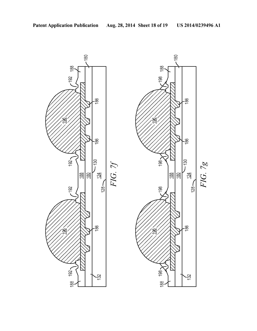
Semiconductor Device and Method of Forming Micro-Vias Partially Through Insulating Material Over Bump Interconnect Conductive Layer for Stress Relief - diagram, schematic, and image 19
Back to Semiconductor Device and Method of Forming Micro-Vias Partially Through Insulating Material Over Bump Interconnect Conductive Layer for Stress Relief , All Patents .