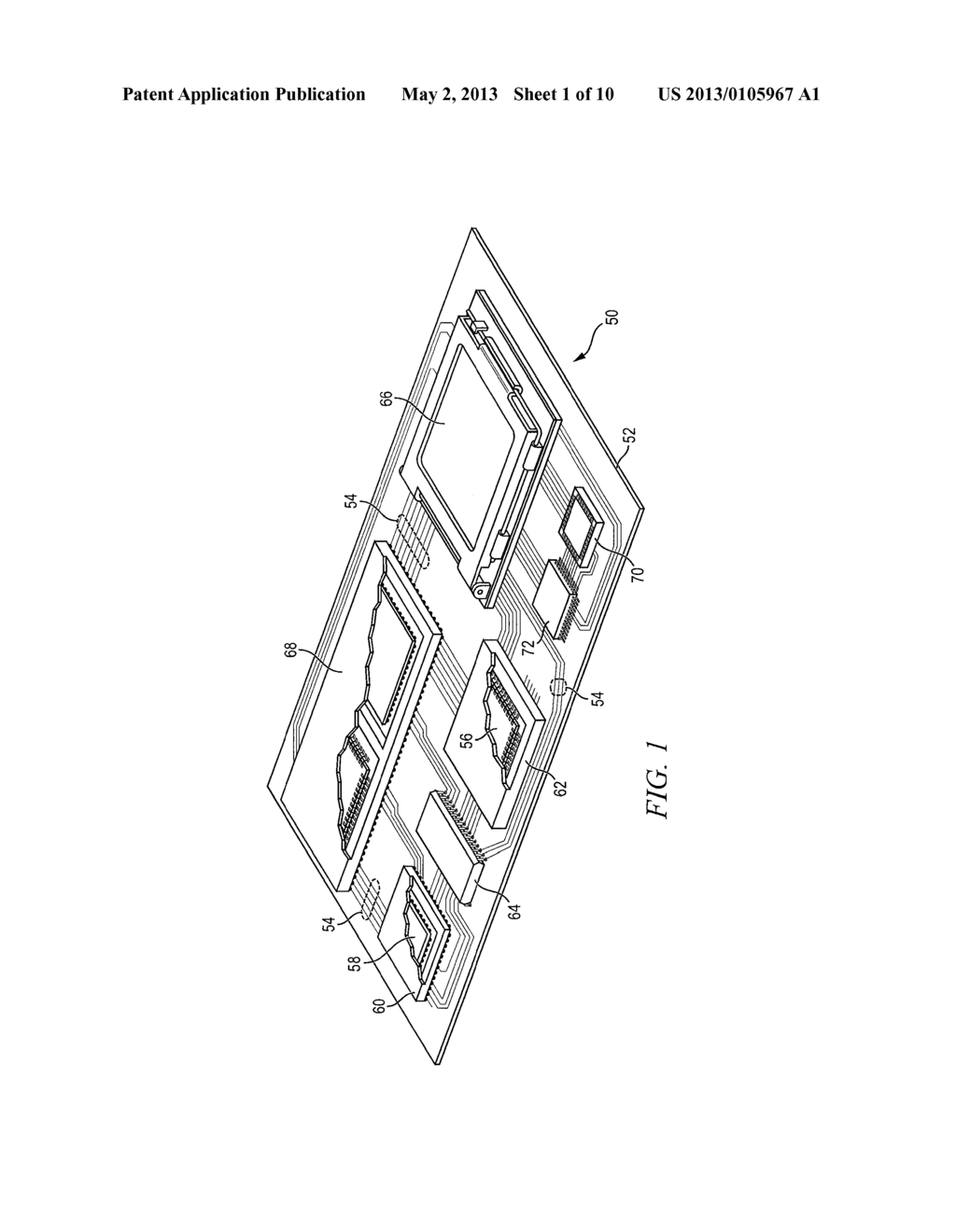
Semiconductor Die and Method of Forming Sloped Surface in Photoresist Layer to Enhance Flow of Underfill Material Between Semiconductor Die and Substrate - diagram, schematic, and image 02
Back to Semiconductor Die and Method of Forming Sloped Surface in Photoresist Layer to Enhance Flow of Underfill Material Between Semiconductor Die and Substrate , All Patents .