Patent application title: COMPOSITE CARRIER FOR WARPAGE MANAGEMENT
Inventors:
IPC8 Class: AH01L2300FI
USPC Class:
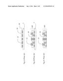
428213
Class name: Structurally defined web or sheet (e.g., overall dimension, etc.) including components having same physical characteristic in differing degree thickness (relative or absolute)
Publication date: 2016-09-01
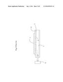
Patent application number: 20160254233
Abstract:
A composite carrier is disclosed for warpage management as a temporary
carrier in semiconductor process. Warpage is reduced for a product,
semi-product, or build-up layer processed on the temporary composite
carrier which is peeled off the temporary carrier in a later step. The
composite carrier comprises a top substrate and a bottom substrate, an
adhesive layer is configured in between the top substrate and a bottom
substrate. One of the embodiments discloses the top substrate of the
composite carrier having a lower CTE and the bottom substrate of the
composite carrier having a higher CTE.Claims:
1. A composite carrier for warpage management, comprises: a top
substrate, selected from a group consisting of Invar (1 ppm), silicon
(Si, .about.3 ppm), Cemented Carbide (.about.5.5 ppm), Alumina (Al,
.about.7.2 ppm), Titanium (Ti, .about.8.6 ppm), glass (0.about.10 ppm),
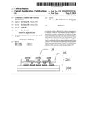
copper clad laminate (CCL, 1.about.17 ppm), stainless steel (10.about.18
ppm), alloy 42 (.about.4.8 ppm), Aluminum Oxide (Al2O3, .about.7 ppm),
Aluminum Nitride (AlN, .about.5 ppm), and Zirconia (ZrO2, .about.10.5
ppm); a bottom substrate, selected from a group consisting of Invar (1
ppm), silicon (Si, .about.3 ppm), Cemented Carbide (.about.5.5 ppm),
Alumina (Al, .about.7.2 ppm), Titanium (Ti, .about.8.6 ppm), glass
(0.about.10 ppm), copper clad laminate (CCL, 1.about.17 ppm), stainless
steel (10.about.18 ppm), alloy 42 (.about.4.8 ppm), Aluminum Oxide
(Al2O3, .about.7 ppm), Aluminum Nitride (AlN, .about.5 ppm), and Zirconia
(ZrO2, 18 10.5 ppm); configured on bottom of the top substrate; and an
adhesive layer, configured between the top substrate and the bottom
substrate; wherein a top of the top substrate provides area for
semiconductor process thereon.
2. A composite carrier for warpage management as claimed in claim 1, wherein a thickness of the top substrate equals to a thickness of the bottom substrate.
3. A composite carrier for warpage management as claimed in claim 1, wherein a thickness of the top substrate is thinner than a thickness of the bottom substrate.
4. A composite carrier for warpage management as claimed in claim 1, wherein a thickness of the top substrate is thicker than a thickness of the bottom substrate.
5. A composite carrier for warpage management as claimed in claim 1, wherein one of the top substrate and the bottom substrate has a CTE around 1.about.4 ppm; and the other one has a CTE around 4.5.about.18 ppm.
6. A composite carrier for warpage management as claimed in claim 1, wherein one of the top substrate and the bottom substrate is made of a material selected from a group consisting of Invar (.about.1 ppm), Silicon (.about.3 ppm), and Glass (1.about.4 ppm); and the other one substrate is made of a material selected from a group consisting of Alloy 42 (.about.4.8 ppm), Aluminum Nitride (AlN, .about.5 ppm), Cemented Carbide (.about.5.5 ppm), Alumina (Al, .about.7.2 ppm), Aluminum Oxide (Al2O3, .about.7 ppm), Titanium (Ti, .about.8.6 ppm), Zirconia (ZrO2, .about.10.5 ppm), glass (0.about.10 ppm), and Stainless Steel (10.about.18.0 ppm).
7. A composite carrier for warpage management as claimed in claim 6, wherein a thickness of the top substrate equals to a thickness of the bottom substrate.
8. A composite carrier for warpage management as claimed in claim 6, wherein a thickness of the top substrate is thinner than a thickness of the bottom substrate.
9. A composite carrier for warpage management as claimed in claim 7, wherein a thickness of the top substrate is thicker than a thickness of the bottom substrate.
Description:
BACKGROUND
[0001] 1. Technical Field
[0002] The present invention relates to a temporary carrier used in a semiconductor process, especially for a composite carrier used as a temporary carrier for warpage management in a semiconductor process.
[0003] 2. Description of Related Art
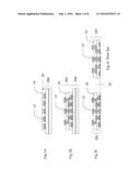
FIGS. 1A.about.1C Show a Prior Art
[0004] FIG. 1 A shows that a build-up layer 10 is processed on top of a traditional carrier 1. The build-up layer process is taken as an example only. A different product or semi-product such as multi-chip package (not shown) can also be processed on top of the temporary carrier 1. In a later step, the processed product or semi-product is torn off the temporary carrier 1 for a further process.
[0005] FIG. 1B shows more build-up layers 10 have been made to form a second build-up layer 105. Both the carrier 1 and the build-up layer 105 experience expansion and shrinkage during semiconductor process, and warpage occurs due to a mismatch in Coefficient of Thermal Expansion (CTE) between the build-up layer 105 and the carrier 1.
[0006] FIG. 1C shows the build-up layer 10 detached from the carrier 1. The detached build-up layer 10 has been distorted. Such a distortion causes problems in registration in a later process for the product.
FIG. 2 Shows a Prior Art
[0007] FIG. 2 shows a prior art--U.S. Pat. No. 8,893,378, a temporary carrier 1 is sucked by a vacuum system to keep the temporary carrier 1 to be in a flat and from being distorted during semiconductor process with heating and cooling. A build-up layer, for example, can be processed on top of the temporary carrier 1. FIG. 2 shows that a cross-section view illustrating the principle of the prior art. A temporary carrier 1 is placed on an evacuable jig 3. The evacuable jig 3 has apertures Sand a gas passage 7. The gas passage 7 is coupled to an evacuation device 9 such as a vacuum pump. The vacuum pump 9 sucks to keep the temporary carrier 1 flat all the time during semiconductor process. The prior art system designed for overcoming the CTE mismatch problem is expensive and complicated because it needs at least an evacuation device 9 and a jig 3. The additional equipment occupies large space which is unacceptable for conventional equipment in semiconductor process. A simple and easy handling method or device compatible with current equipment for a temporary carrier's warpage management is a long desirable solution in semiconductor industry.
BRIEF DESCRIPTION OF THE DRAWINGS
[0008] FIGS. 1A.about.1C show a prior art
[0009] FIG. 2 shows a prior art
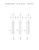
[0010] FIGS. 3A.about.3C show build-up layers processed on the composite carrier
[0011] FIG. 4A shows a first embodiment of the composite carrier according to the present invention
[0012] FIG. 4B shows a second embodiment of the composite carrier according to the present invention
[0013] FIG. 4C shows a third embodiment of the composite carrier according to the present invention
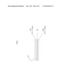
[0014] FIG. 5 shows a fourth embodiment of the composite carrier according to the present invention
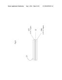
[0015] FIG. 6 shows a fifth embodiment of the composite carrier according to the present invention
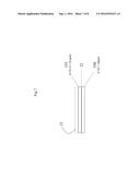
[0016] FIG. 7 shows a sixth embodiment of the composite carrier according to the present invention
[0017] FIGS. 8A.about.8C show modified embodiments according to the present invention.
DETAILED DESCRIPTION OF THE INVENTION
[0018] A temporary composite carrier is disclosed for warpage management in semiconductor process according to the present invention. Warpage is reduced for a Product, semi-product, or build-up layer processed on top of the temporary composite carrier according to the present invention. The temporary composite carrier according to the present invention has a sandwich structure which comprises a top substrate, a bottom substrate, and an adhesive layer. The adhesive layer is configured in between the top substrate and a bottom substrate for combining the substrates tight together. One of the embodiments discloses that the top substrate has a lower CTE and the bottom substrate has a higher CTE.
[0019] A first advantage for the present invention is that the composite carrier is a safe carrier to prevent chamber contamination if breakage occurs. No debris or only very little debris shall come off to contaminate the chamber, because any debris from breakage of one or both of the substrates shall be adhered to the adhesive layer.
[0020] A second advantage for the present invention is that the temporary composite carrier has a top substrate and a bottom substrate which can be with different CTE. For example, the top substrate is made of a material with a relative lower CTE and the bottom substrate is made of a material with a relative higher CTE. When a product, semi-product, or build-up layer is processed on top of the top substrate and with a higher CTE relative to the top substrate of the composite carrier, a stress of the bottom substrate shall offset at least partial stress from the one processed on the top substrate to reduce warpage of the top substrate as well as the one processed on top.
[0021] A third advantage for the present invention is that the top substrate and the bottom substrate may choose different thickness for a better stress matching in a specific case. Because in most cases, a mismatch in mechanical properties, such as CTE, between a temporary carrier and a product processed on top of the temporary carrier always exists. Based on the adjustable thickness, in combination of different CTE chosen for either one of the two substrates according to the present invention, the temporary composite carrier can be tailored to minimize the stress and warpage of the total structure, especially of the product, semi-product, or build-up layer . . . etc., processed on top.
FIGS. 3A.about.3C Show Build-Up Layers Processed on the Composite Carrier
[0022] FIG. 3A shows a build-up layer 20 made on top of a top substrate of the composite carrier 200.
[0023] FIG. 3B shows more build-up layers 20 have been made to form a second build-up layer 205. The composite carrier 200 experiences shrinkage and warpage after thermal shock during semiconductor process and due to the CTE mismatch between the build-up layer 20 and the composite carrier 200. However, FIG. 3B shows only very little warpage due to a stress of the bottom substrate of the composite carrier 200.
[0024] Build-up layer is taken as an example. Copper line 15 in the build-up layer roughly has a CTE around 17 ppm, and dielectric layer 16 in the build-up layer such as one of Polybenzoxazole (PBO), Polyimide (PI), or Benzocyclobuten (BCB), roughly has a CTE around 30 ppm; in combination the build-up layer 205 roughly has a CTE around 20 ppm.
[0025] The bottom substrate 21B is made of a material having a CTE larger than a CTE of the top substrate 21T so that a stress from the bottom substrate is able to offset some stress of the build-up layer 205 on top so that the warpage of the build-up layer 205 is reduced before or after it being detached from the temporary composite carrier 200.
[0026] FIG. 3C shows the build-up layer 205 detached from the carrier 200. The detached build-up layer 205 has very little distortion as compared with the build-up layer 105 fabricated on a traditional carrier 1.
[0027] Further referring to FIG. 3C, compared with FIG. 1C, the traditional build-up layer 105 has a distortion as indicated as distance 24. The build-up layer 205 of FIG. 3C according to the present invention has significant less distortion than the traditional build-up layer 105 of FIG. 1C.
FIG. 4A Shows a First Embodiment of the Composite Carrier According to the Present Invention
[0028] FIG. 4 shows a composite carrier 200 which comprises a top substrate 21T, an adhesive layer 22 is configured on bottom of the top substrate 21T, and a bottom substrate 21B is configured on bottom of the adhesive layer 22. The top substrate 21T is made of a material selected from a group consisting of silicon, glass, copper clad laminate (CCL), silicon carbide (SiC), stainless steel, alloy 42, and ceramic including Aluminum Oxide (Al2O3, .about.7 ppm), Aluminum Nitride (AlN, .about.5 ppm), and Zirconia (ZrO2, .about.10.5 ppm). The bottom substrate 21B is made of a material selected from a group consisting of silicon, glass, copper clad laminate (CCL), silicon carbide (SiC), stainless steel, alloy 42, and ceramic. A top area 23 of the top substrate 21T provides area for semiconductor process thereon.
[0029] No debris or only very little debris shall come off from the composite carrier 200 to contaminate the chamber, because any debris from breakage of one or both of the substrates of the composite carrier 200 shall adhere to the adhesive layer 22.
FIG. 4B Shows a Second Embodiment of the Composite Carrier According to the Present Invention
[0030] FIG. 4B shows that a composite carrier 201 has a top substrate 21T and a bottom substrate 31B. An adhesive layer is configured in between the top substrate 21T and the bottom substrate 31B. A thickness of the bottom substrate 31B is thicker than a thickness of the top substrate 21T. The higher thickness of the bottom substrate 31B provides higher stiffness to withstand the bending or distortion for the product being processed on top 23 of the top substrate 21T.
FIG. 4C Shows a Third Embodiment of the Composite Carrier According to the Present Invention
[0031] FIG. 4C shows that a composite carrier 202 has top substrate 31T and a bottom substrate 21B. A thickness of the top substrate 31T is thicker than a thickness of the bottom substrate 21B. The higher thickness of the top substrate 31T provides higher stiffness to withstand the bending or distortion for the product being processed on top 23 of the top substrate 31T.
FIG. 5 Shows a Fourth Embodiment of the Composite Carrier According to the Present Invention
[0032] FIG. 5 shows a composite carrier for warpage management. FIG. 5 shows either one of the top substrate 35T or the bottom substrate 35B is made of a material having a CTE around 1.about.18 ppm. The material of the top substrate 35T can be the same as the material of the bottom substrate 35B. Alternatively, the material of the top substrate 35T can be different from the material of the bottom substrate 35B.
[0033] The material for the substrate can be used is one selected from the group consisting of:
[0034] Invar having a CTE around 1 ppm,
[0035] Aluminum Nitride having a CTE around 5 ppm,
[0036] Silicon having a CTE around 3 ppm,
[0037] Glass having a CTE around 4 ppm,
[0038] Alloy 42 having a CTE around 4.8 ppm,
[0039] Cemented Carbide having a CTE around 5.5 ppm,
[0040] Aluminum Oxide having a CTE around 7 ppm,
[0041] Alumina having a CTE around 7.2 ppm,
[0042] Titanium having a CTE around 8.6 ppm,
[0043] Zirconia having a CTE around 10.5 ppm,
[0044] Glass having a CTE around 0.about.10 ppm, and
[0045] Stainless Steel having a CTE around 10.about.18.0 ppm.
FIG. 6 Shows a Fifth Embodiment of the Composite Carrier According to the Present Invention
[0046] FIG. 6 shows that the material of the top substrate 35T is different from the material of the bottom substrate 35B. The material of the top substrate 35T is selected from a material having CTE from 1.about.4 ppm; and the material of the bottom substrate 35B is selected from a material having a CTE from 4.5.about.18 ppm.
FIG. 7 Shows a Sixth Embodiment of the Composite Carrier According to the Present Invention
[0047] FIG. 7 shows that the material of the top substrate 35T is different from the material of the bottom substrate 35B. The material of the top substrate 35T is selected from a material having CTE from 4.5.about.18 ppm; and the material of the bottom substrate 35B is selected from a material having a CTE from 1.about.4 ppm.
[0048] FIGS. 8A.about.8C show modified embodiments according to the present invention.
[0049] FIG. 8A shows polymer 38 wrapping around a peripheral side of the top substrate 35T and the bottom substrate 35B of the composite carrier to enhance the rigidity of the composite substrate. The polymer 38 has a thickness h equivalent to the thickness t of the composite substrate. The polymer 38 protrudes out smoothly in a direction parallel with a surface of the substrate.
[0050] FIG. 8B shows a flat chamfer 392 is made on the corner of the substrate 35T, 35B.
[0051] FIG. 8C shows a curve chamfer 393 is made on the corner of the substrate 35T, 35B.
[0052] While several embodiments have been described by way of example, it will be apparent to those skilled in the art that various modifications may be configured without departs from the spirit of the present invention. Such modifications are all within the scope of the present invention, as defined by the appended claims.
User Contributions:
Comment about this patent or add new information about this topic:

