Patent application title: STATIC CURRENT IN IO FOR ULTRA-LOW POWER APPLICATIONS
Inventors:
Mukesh Nair (Bangalore, IN)
Assignees:
NXP B.V.
IPC8 Class: AH02H904FI
USPC Class:
361 56
Class name: Safety and protection of systems and devices load shunting by fault responsive means (e.g., crowbar circuit) voltage responsive
Publication date: 2015-03-19
Patent application number: 20150077887
Abstract:
An input/output (IO) circuit including: an IO driver circuit; an
electrostatic discharge (ESD) protection semiconductor switch with a
first input configured to receive an ESD, a second input connected to an
ESD rail, and a switch control input; an ESD trigger circuit connected to
the switch control input, wherein the ESD trigger circuit is configured
to produce a trigger signal to close the protection semiconductor switch
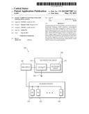
when the ESD detection circuit detects an ESD; and a bias circuit
configured to provide a back bias signal to an isolated well of the ESD
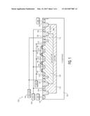
protection semiconductor switch when IO circuit is in normal operation.Claims:
1. An input/output (IO) circuit comprising: an IO driver circuit; an
electrostatic discharge (ESD) protection semiconductor switch with a
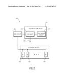
first input configured to receive an ESD, a second input connected to an
ESD rail, and a switch control input; an ESD trigger circuit connected to
the switch control input, wherein the ESD trigger circuit is configured
to produce a trigger signal to close the protection semiconductor switch
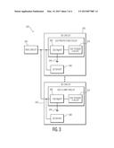
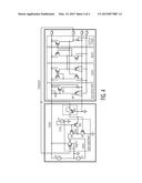
when the ESD detection circuit detects an ESD; and a bias circuit
configured to provide a back bias signal to an isolated well of the ESD
protection semiconductor switch when IO circuit is in normal operation.
2. The circuit of claim 1, wherein the ESD protection semiconductor switch is an NMOS device and the back bias signal is negative relative to a ground.
3. The circuit of claim 2, wherein the back bias signal is applied to an isolated p-well (IPW) of the ESD protection semiconductor switch.
4. The circuit of claim 2, wherein the ESD trigger circuit includes an output semiconductor switch connected between the ESD trigger circuit and switch control input, wherein the output semiconductor switch is configured to isolate the ESD trigger circuit from the negative back bias signal.
5. The circuit of claim 2, wherein the ESD protection circuit includes an input semiconductor switch connected between the isolated well and ground, wherein the input semiconductor switch is configured to prevent the connection of the back bias signal to a ground during normal operation of the integrated circuit.
6. The circuit of claim 1, wherein the IO driver circuit further comprises an IO semiconductor driver wherein the IO semiconductor driver receives the back bias signal when the IO driver circuit is in an idle state.
7. The circuit of claim 6, wherein the protection semiconductor switch and the IO semiconductor driver are NMOS devices and the back bias signal is negative relative to a ground and wherein the back bias signal is applied to an isolated p-well (IPW) of the driver device.
8. The circuit of claim 6, wherein the protection semiconductor switch and the IO semiconductor driver are PMOS devices and the back bias is positive relative to the supply connected to the source and wherein the back bias is applied to an isolated n-well of the driver device
9. The circuit of claim 1, wherein the ESD rail is a ground.
10. The circuit of claim 1, wherein the bias circuit is external to the IO circuit.
11. A method of back biasing an electrostatic discharge protection semiconductor switch having an isolated well in an IO circuit comprising: applying a back bias signal to the isolated well of the ESD protection semiconductor switch during normal integrated circuit operation; detecting an ESD; generating an ESD trigger signal; applying the ESD trigger signal to the ESD protection switch to open the ESD protection switch to connect the ESD to an ESD rail; and grounding the isolated well when the ESD is detected.
12. The method of claim 11, further comprising back biasing an IO semiconductor driver when the IO semiconductor is idle.
13. The method of claim 11, wherein the ESD protection semiconductor switch is an NMOS device and the back bias signal is negative relative to the ground.
14. The method of claim 13, wherein the isolated well is an isolated p-well (IPW) and the back bias signal is applied to the IPW of the ESD protection semiconductor switch.
15. The method of claim 13 further comprising protecting the trigger signal from the negative back bias signal.
16. The method of claim 13 further comprising preventing the connection of the back bias signal to ground during normal operation of the integrated circuit.
17. An input/output (IO) circuit comprising: an IO driver circuit; an electrostatic discharge (ESD) protection semiconductor switch having an isolated p-well (IPW) node, wherein the ESD protection semiconductor switch is connected between a voltage source and a ground configured to connect the ESD to the ground, wherein in the ESD protection semiconductor switch is an NMOS device; an ESD trigger circuit connected to a gate of the ESD protection semiconductor switch, wherein the ESD trigger circuit is configured to produce a trigger signal to close the ESD protection semiconductor switch when the ESD detection circuit detects an ESD; a bias voltage source configured to produce a negative back bias signal; a bias voltage semiconductor switch connected between the bias voltage source and the ESD protection semiconductor switch, wherein the bias voltage semiconductor switch is configured to control the application of the back bias signal to the IPW node; and an IPW node grounding semiconductor switch connected between the IPW node and the ground, wherein the IPW node grounding semiconductor switch is configured to connect the IPW node to ground based upon the trigger signal indicating the ESD.
18. The circuit of claim 17, further comprising a IPW node protection semiconductor switch connected between the drain and gate of the IPW node grounding semiconductor switch, wherein the IPW node protection semiconductor switch is configured to place the IPW node grounding semiconductor switch in a diode configuration.
19. The circuit of claim 18, further comprising ESD trigger circuit protection semiconductor switch connected between the ESD trigger circuit and the gate of the IPW node grounding semiconductor switch.
20. The circuit of claim 19, further comprising a control voltage source connected to the gates of the bias voltage semiconductor switch and node protection semiconductor switch.
Description:
TECHNICAL FIELD
[0001] Various exemplary embodiments disclosed herein relate generally to IO for ultra-low power applications.
BACKGROUND
[0002] As devices are scaled down static leakage increases and is becoming significant in ultra-low power applications. ESD devices are not active when the circuit is operating and are a source of current leakage. To put a switch in place to switch out the ESD devices may almost double the size and cost of the overall circuit.
SUMMARY
[0003] A brief summary of various exemplary embodiments is presented below. Some simplifications and omissions may be made in the following summary, which is intended to highlight and introduce some aspects of the various exemplary embodiments, but not to limit the scope of the invention. Detailed descriptions of an exemplary embodiment adequate to allow those of ordinary skill in the art to make and use the inventive concepts will follow in later sections.
[0004] Various exemplary embodiments relate to an input/output (IO) circuit including: an IO driver circuit; an electrostatic discharge (ESD) protection semiconductor switch with a first input configured to receive an ESD, a second input connected to an ESD rail, and a switch control input; an ESD trigger circuit connected to the switch control input, wherein the ESD trigger circuit is configured to produce a trigger signal to close the protection semiconductor switch when the ESD detection circuit detects an ESD; and a bias circuit configured to provide a back bias signal to an isolated well of the ESD protection semiconductor switch when IO circuit is in normal operation.
[0005] Further, various exemplary embodiments relate to a method of back biasing an electrostatic discharge protection semiconductor switch having an isolated well in an IO circuit including: applying a back bias signal to the isolated well of the ESD protection semiconductor switch during normal integrated circuit operation; detecting an ESD; generating an ESD trigger signal; applying the ESD trigger signal to the ESD protection switch to open the ESD protection switch to connect the ESD to an ESD rail; and grounding the isolated well when the ESD is detected.
[0006] Further, various exemplary embodiments relate to an input/output (IO) circuit including: an IO driver circuit; an electrostatic discharge (ESD) protection semiconductor switch having an integrated p-well (IPW) node, wherein the ESD protection semiconductor switch is connected between a voltage source and a ground configured to connect the ESD to the ground, wherein in the ESD protection semiconductor switch is an NMOS device; an ESD trigger circuit connected to a gate of the ESD protection semiconductor switch, wherein the ESD trigger circuit is configured to produce a trigger signal to close the ESD protection semiconductor switch when the ESD detection circuit detects an ESD; a bias voltage source configured to produce a negative back bias signal; a bias voltage semiconductor switch connected between the bias voltage source and the ESD protection semiconductor switch, wherein the bias voltage semiconductor switch is configured to control the application of the back bias signal to the IPW node; and an IPW node grounding semiconductor switch connected between the IPW node and the ground, wherein the IPW node grounding semiconductor switch is configured to connect the IPW node to ground based upon the trigger signal indicating the ESD.
BRIEF DESCRIPTION OF THE DRAWINGS
[0007] In order to better understand various exemplary embodiments, reference is made to the accompanying drawings, wherein:
[0008] FIG. 1 illustrates a cross-sectional view of an embodiment in accordance with the invention of a BigFET 100 that may be used in an ESD circuit;
[0009] FIG. 2 illustrates an embodiment in accordance with the invention of an integrated circuit with centralized ESD protection for the IO circuits;
[0010] FIG. 3 illustrates an embodiment in accordance with the invention of an integrated circuit with a distributed ESD protection for the IO circuits; and
[0011] FIG. 4 illustrates an embodiment in accordance with the invention of an ESD protection circuit and an ESD trigger circuit.
[0012] To facilitate understanding, identical reference numerals have been used to designate elements having substantially the same or similar structure and/or substantially the same or similar function.
DETAILED DESCRIPTION
[0013] The description and drawings illustrate the principles of the invention. It will thus be appreciated that those skilled in the art will be able to devise various arrangements that, although not explicitly described or shown herein, embody the principles of the invention and are included within its scope. Furthermore, all examples recited herein are principally intended expressly to be for pedagogical purposes to aid the reader in understanding the principles of the invention and the concepts contributed by the inventor(s) to furthering the art, and are to be construed as being without limitation to such specifically recited examples and conditions. Additionally, the term, "or," as used herein, refers to a non-exclusive or (i.e., and/or), unless otherwise indicated (e.g., "or else" or "or in the alternative"). Also, the various embodiments described herein are not necessarily mutually exclusive, as some embodiments can be combined with one or more other embodiments to form new embodiments. As used herein, the terms "context" and "context object" will be understood to be synonymous, unless otherwise indicated.
[0014] Current integrated circuits (ICs) may include many input/output (IO) pins. Some ICs may include a hundred or more pins. An IO circuit may be associated with each IO pin to control and drive the IO of the pin. As these IO pins are exposed to the environment, especially while being transported and handled during manufacturing, they are subject to electrostatic discharge (ESD). ESD may result in very short high voltage signal being present at the IO pin. As a result ESD protection circuits may be implemented at each IO pin to protect the IO and other internal IC circuitry from being damaged by ESD.
[0015] Such ESD protection circuitry typically includes an ESD detector and trigger and an ESD protection semiconductor switch. The ESD detector and trigger detects the presence of ESD and generates a trigger signal that opens the ESD protection semiconductor switch. Because of the high charge (current) involved in ESD the ESD protection semiconductor switch may be a large field effect transistor (BigFET). Such a BigFET may have a static leakage current of up to 3 μA. In an IC that may have, for example, 100 IO pins and hence potentially 100 ESD switches protecting these pins, the total leakage current may be 0.3 mA. In today's low power and ultra-low power ICs, a 0.3 mA leakage current is a significant power draw that degrades the performance of the IC. Accordingly, there remains a need to reduce the static current draw of ESD protection circuits. In addition, the IO driver circuit may also include one or more large semiconductor transistors that may also be idle at times resulting additional large static currents.
[0016] The ESD protection circuits may be implemented as a centralized ESD system or as a distributed ESD system. In the centralized ESD system a few ESD protection circuits are used in the IC to protect the IO of the IC from ESD. In a distributed ESD system, each IO pin and its associated IO drivers may have an ESD protection circuit. Both types will be discussed below.
[0017] In the embodiments described below, the static current of the ESD protection semiconductor switches, which are BigFETs, are reduced by applying a back bias. In the example described above for a BigFET with a 3 μA static leakage current, the application of a 1V back bias may reduce the static current leakage to 150 nA. This is a 20× reduction in static leakage current. In the example of an IC with 100 ESD protection circuits, the total static leakage current due to the BigFETs found in the ESD protection circuits may be reduced from 300 μA to 15 μA.
[0018] FIG. 1 illustrates a cross-sectional view of an embodiment in accordance with the invention of a BigFET 100 that may be used in an ESD circuit. Also, such a BigFET 100 may also be found in the IO driver circuits. The illustrated BigFET 100 is an NMOS device. The BigFET 100 includes a P-substrate 105, a deep N-well (NW) region 110 that includes a N.sup.+ guard region 115, and an isolated P-well (IPW) 120. The BigFET further includes N.sup.+ doped regions 125 inside the IPW 120 and N.sup.+ doped regions 130 over the deep NW region 110. The alternating N.sup.+ doped regions 125, 126 form the source and the drain the BigFET 100. Further, the BigFET includes P.sup.+ doped regions 135 inside the IPW 120 and P.sup.+ doped regions 140 over the P-substrate 105. The BigFET also includes gate electrodes 145 formed on gate regions of the IPW 120 between the N.sup.+ doped regions 125. A voltage applied to the gate electrodes 145 may cause the BigFET 100 to turn on and to allow current to flow between the source and the drain. A voltage VDDE 150 may be applied to the drain of the BigFET 100, and the source of the BigFET 100 may be connected to a ground GNDE 155. A bias generator 160 applies a bias voltage to the P.sup.+ doped regions 135 in order to apply a back bias on the IPW 120. As described above, such a voltage may greatly decrease the static current leakage of the BigFET.
[0019] Most ESD protection circuits use NMOS BigFETs, so a negative back bias voltage is needed. The use of a negative back bias voltage with respect to the source complicates the IO circuit structure as the other circuit elements of the IO circuit may need to be isolated from the negative back bias voltage. If instead a PMOS BigFET is used in the ESD protection circuit, then a positive back bias voltage may be used.
[0020] FIG. 2 illustrates an embodiment in accordance with the invention of an integrated circuit with centralized ESD protection for the IO circuits. The integrated circuit 200 includes an ESD protection circuit 205, a bias circuit 220 (which could also be reused from other portions within the IC), and IO driver circuits 230. In the IC 200 the ESD protection circuit 205 is centrally located. Also, there may be more than one centrally located ESD protection circuit 205 depending upon the size and geometry of the IC 200. The ESD protection circuit 205 includes an ESD BigFET 210 and ESD trigger circuit 215. The ESD BigFET 210 may be an NMOS device as described in FIG. 1 or a PMOS device depending in various design parameters. In either case the BigFET is designed to be able to handle a specified level of ESD. The ESD trigger circuit 215 detects ESD in the IC, especially ESD present at the IO of the IC 200. When the trigger circuit 215 detects ESD, the trigger circuit 215 produces a trigger signal to switch and open the ESD BigFET 210 in order to conduct the ESD to ground 240. Further the ESD may be conducted to a common rail. The ground 240 or the common rail may be called an ESD rail in order to refer to both embodiments.
[0021] The bias circuit 220 may provide a bias signal to the ESD BigFET 210 when the IC is in normal operation. Normal operation for purposes of this description is any operation of the IC other than ESD operation. The bias signal back biases the ESD BigFET 210 in order to reduce the static leakage current of the ESD BigFET 210. As discussed above, the bias signal may have a negative or positive voltage relative to ground depending on whether the BigFET 210 is an NMOS (negative bias) or PMOS (positive bias) device. The bias circuit 220 an ESD protection circuit 205 may include specific isolating and control elements in order to control the application of the bias signal during normal operation of the IC 200 as well as during ESD. An example of a more detailed embodiment in accordance with the invention for these circuits will be described below in FIG. 4.
[0022] The IO driver circuits 230 may also include a large semiconductor conductor transistor. Such large semiconductor transistors may also be back biased when not active in order to reduce their static leakage current. Accordingly the bias circuit 220 may also provide a bias signal to the IO driver circuits 230. The IO driver circuit 230 also has an enable pin that receives a control signal to enable and disable the IO driver circuit 230 and hence the IO pin. The control signal applied to the enable pin of the IO driver circuit 230 may also be used to apply the bias signal to the large semiconductor transistor in the IO driver circuit 230 when the IO driver circuit 230 is idle.
[0023] FIG. 3 illustrates an embodiment in accordance with the invention of an integrated circuit with a distributed ESD protection for the IO circuits. The integrated circuit 300 includes a number of IO circuits 335 and a bias circuit 320. The IO circuit 335 includes an ESD protection circuit 305, and an IO driver circuit 330. The ESD protection circuit 305 includes an ESD BigFET 310 and ESD trigger circuit 315. The ESD BigFET 310 may be an NMOS device as described in FIG. 1 or a PMOS device depending in various design parameters. In either case the BigFET is designed to be able to handle a specified level of ESD. The ESD trigger circuit 315 detects ESD in the IC, especially ESD present at the IO of the IC 300. When the trigger circuit 315 detects ESD, the trigger circuit 315 produces a trigger signal to switch and open the ESD BigFET 310 in order to conduct the ESD to ground 340 or to a common rail
[0024] The bias circuit 320 provides a bias signal to the ESD BigFETs 310 when the IC is in normal operation. The bias signal back biases the ESD BigFETs 310 in order to reduce the static leakage current of the ESD BigFETs 310. As discussed above, the bias signal may have a negative or positive voltage relative to ground depending on whether the BigFET 310 is an NMOS (negative bias) or PMOS (positive bias) device. The bias circuit 320 and ESD protection circuit 305 may include specific isolating and control elements in order to control the application of the bias signal during normal operation of the IC 300 as well as during ESD. An example of a more detailed embodiment in accordance with the invention for these circuits will be described below in FIG. 4.
[0025] The IO driver circuits 330 may also include a large semiconductor conductor transistor. Such large semiconductor transistors may also be back biased in order to reduce their static leakage current. Accordingly the bias circuit 320 may also provide a bias signal to the IO driver circuits 330. The IO driver circuit 330 also has an enable pin that receives a control signal to enable and disable the IO driver circuit 330 and hence the IO pin. The control signal applied to the enable pin of the IO driver circuit 330 may also be used to apply the bias signal to the large semiconductor transistor in the IO driver circuit 330 when the IO driver circuit 330 is idle.
[0026] The bias circuit 220, 320 may be either internal or external to the IC 200. In situations where the bias circuit cannot easily be implemented internally to the IC, the IC may include an additional IO that receives an external bias signal from an external bias circuit. The use of an external bias circuit does result in an additional IO that needs to have ESD protection as well. Further, the bias rail would need to be thicker because it is subject to ESD due to the external connection. Further, if the external bias circuit generates a negative bias signal, the IO for the bias signal may not be able to use normal MOS transistors due to the negative voltage, thus other types of transistors such as Grounded Gate NMOS Transistor (GGNMOST) or low voltage triggered configurations (LVTSCR) structure using a parasitic bipolar may be needed. Also, a negative voltage would have to be generated externally when the bias signal needs to be applied to a NMOS BigFET. Further, when a bias signal is used there may be a bit of a delay in overcoming the effect of the back bias signal if applied to IO drivers, so the timing of the turning on the IO drives needs to account for such a delay. Also, the external bias circuit may be used with either the centralized or distributed ESD system.
[0027] FIG. 4 illustrates an embodiment in accordance with the invention of an ESD protection circuit and an ESD trigger circuit. The ESD protection circuit 400 includes a reverse body bias (RBB) circuit 405 and an ESD trigger circuit 410. The ESD trigger circuit further includes a detection circuit 415, a hold circuit 420, a reset circuit 425, and an output stage circuit 430. The detection circuit 415 detects an ESD and produces a signal. The produced signal will be present for a certain time based upon a time constant based upon the resistor R8 and transistor MN15. The hold circuit 420 holds the signal produced by the detection circuit 415. The reset circuit 425 determines when the ESD has finished and resets the trigger circuit 410 to an off state. The output stage circuit 430 includes a drive circuit to output the ESD trigger signal for use by other circuits.
[0028] The RBB 405 includes the BigFET transistor MN0. BigFET MN0 when turned on and opened provides a path for the ESD when present. BigFET MN0 includes an IPW substrate that has an IPW node where a bias signal may be applied to the IPW substrate to back bias the BigFET MN0. The source of BigFET MN0 is connected to ground GND, the drain to VDDE, and the gate to the ESD trigger signal TRIG. A voltage source V0 supplies the voltage VDDE to the various circuit elements, which in this example is 3V. A voltage source V1 provides the bias voltage BIAS to back bias the BigFET MN0. In this example, the bias voltage has a value of -1V.
[0029] MN1 and MN2 are transistors that control the voltage applied to the node IPW that provides the bias to IPW of BigFET MN0. The drain of MN2 is connected to the voltage source V1 (negative with respect to ground) and receives the BIAS signal. The source of MN2 is connected to the node IPW, and the gate is connected to a voltage source V2 that produces a control signal CTRL. The voltage source may produce a 1.8V signal that drives the gate of MN2 during the normal operation mode. During ESD both V1 and CTRL may not be present
[0030] The drain of MN1 is connected to the node IPW, and the source is connected to ground GND. The gate of MN1 receives the ESD trigger signal TRIG via a transistor MP1. A further transistor MN3 has a source that receives the ESD trigger signal TRIG via a transistor MP1 and a drain connected to the node IPW and hence the drain of MN1. The gate of MN3 is driven by the control signal CTRL. MN3 causes MN1 to be in a diode configuration and this prevents MN1 from turning on due to the negative voltage at IPW due to the negative bias signal BIAS. The transistor MP1 has a source connected to the trigger signal TRIG, a drain connected to the gate of MN1 and the source of MN3, and a gate connected to ground.
[0031] Now the operation of the ESD protection circuit will be described. During ESD operation the ESD trigger circuit 410 will detect the ESD and produce the ESD trigger signal TRIG. The ESD trigger signal TRIG will be applied to gate of BigFET MN0 which will open BigFET MN0 and allow the ESD current to flow through BigFET MN0 to ground or to a common rail. The ESD trigger signal TRIG is also applied to the gate of MN1 via MP1, which connects the node IPW to ground, thus removing the back bias from BigFET MN0 to assure proper operation of the ESD protection circuit.
[0032] During normal operation, the control signal CTRL from V2 turns on both MN2 and MN3. With MN2 on the bias signal BIAS is applied to the node IPW and thus back biases BigFET MN0 in order to reduce the static leakage current of BigFET MN0. With MN3 on, MN1 is placed in a diode configuration and MN1 is off because the gate is driven negative with respect to the source and there is no Vgs (gate to source voltage). With MN1 in a diode configuration the negative voltage of the bias signal BIAS will not turn MN1 on, which would ground the node IPW and thus defeat the back biasing of BigFET MN0. Further, with MN3 on, the negative voltage of the bias signal BIAS is applied back towards the ESD trigger circuit, but MP1 isolates the ESD trigger circuit 410 from the bias signal BIAS during normal operation by being off during normal operation. MP1 remains OFF during normal operation as the drain is driven negative with respect to the gate which is grounded, and the source is connected to ground via the trigger circuit.
[0033] Various aspects of the circuit shown in FIG. 4 result from the fact that the bias signal BIAS is a negative voltage. Such a negative voltage affects other devices where such negative voltage is applied. Accordingly, various additional circuit element, e.g., MN3 and MP1 may be used to isolate and negate the effects of the negative voltage bias signal BIAS.
[0034] The BigFET devices described herein may include isolated wells that may be used to back bias the BigFET devices. If the device is an NMOS device, the isolated well will be an isolated P-well. If the device is a PMOS device, the isolated well will be an isolated N-well.
[0035] It should be appreciated by those skilled in the art that any block diagrams herein represent conceptual views of illustrative circuitry embodying the principles of the invention. Further, in the circuits shown additional elements may also be included as needed, or variations to the structure of the circuit may be made to achieve the same functional results as the circuits illustrated.
[0036] Although the various exemplary embodiments have been described in detail with particular reference to certain exemplary aspects thereof, it should be understood that the invention is capable of other embodiments and its details are capable of modifications in various obvious respects. As is readily apparent to those skilled in the art, variations and modifications can be effected while remaining within the spirit and scope of the invention. Accordingly, the foregoing disclosure, description, and figures are for illustrative purposes only and do not in any way limit the invention, which is defined only by the claims.
User Contributions:
Comment about this patent or add new information about this topic:
Images included with this patent application:
 |  |
 |  |
 |
| Similar patent applications: | |
| Date | Title |
|---|---|
| 2015-03-26 | Synthesis of three-dimensional graphene foam: use as supercapacitors |
| 2015-03-19 | Motor drive with inherent power isolation |
| 2015-03-26 | Grounded belt and movable drawer apparatus |
| 2015-03-26 | Integrated circuit with protection function |
| 2015-02-26 | Solid state fault current limiter |
| New patent applications in this class: | |
| Date | Title |
|---|---|
| 2019-05-16 | Circuit for preventing surge and electronic apparatus having the same |
| 2019-05-16 | Surge protective circuit and surge protective device |
| 2019-05-16 | Apparatuses and method for over-voltage event protection |
| 2019-05-16 | Complex electronic component |
| 2018-01-25 | High voltage clamps with transient activation and activation release control |
| New patent applications from these inventors: | |
| Date | Title |
|---|---|
| 2012-12-20 | Dc-dc converter arrangement |
| 2011-02-10 | Battery charger for a phtovoltaic system, a controller therefor and a method of controlling the same |
| 2008-11-06 | Electronic device |
| Top Inventors for class "Electricity: electrical systems and devices" | |
| Rank | Inventor's name |
|---|---|
| 1 | Zheng-Heng Sun |
| 2 | Levi A. Campbell |
| 3 | Li-Ping Chen |
| 4 | Robert E. Simons |
| 5 | Richard C. Chu |