Patent application title: HEAT SINK DEVICE WITH EMI SHIELDING FUNCTION
Inventors:
Chih-Hao Lin (New Taipei, TW)
Yi-Hsien Lee (New Taipei, TW)
IPC8 Class: AH05K900FI
USPC Class:
165185
Class name: Heat exchange heat transmitter
Publication date: 2015-02-19
Patent application number: 20150047822
Abstract:
A heat sink is configured to dissipate heat generated by an electronic
component and protect the electronic component from Electromagnetic
Interference (EMI). The heat sink comprises a base and a number of
waveguides extending out from the base. A number of through holes is
defined through the base. Each of the waveguides is a hollow but blind
tube communicating with a through hole.Claims:
1. A heat sink for dissipating heat generated by an electronic component
and protecting the electronic component from Electromagnetic Interference
(EMI), the heat sink comprising: a base; a plurality of waveguides
extending from the base; and a plurality of through holes running through
the base; wherein each one of the plurality of waveguides is a hollow
tube communicating with a corresponding one of the plurality of through
holes.
2. The heat sink of claim 1, wherein each waveguide is made of metal, or other thermal conductive materials.
3. The heat sink of claim 1, wherein a receiving cutout is defined in a lower surface of the base and is configured to receive the electronic component.
4. The heat sink of claim 1, wherein one end of each waveguide is open to communicate with a corresponding through hole of the base and another end of each waveguide is closed.
5. The heat sink of claim 1, wherein the base and the waveguide are integrally formed.
Description:
FIELD
[0001] The subject matter herein generally relates to heat sinks.
BACKGROUND
[0002] A conventional heat sink can be mounted on an electronic component for dissipating heat generated by the electronic component. However, electromagnetic interference (EMI) often occurs between neighboring electronic components due to inductive coupling, and the conventional heat sink does not shield the electronic component from external EMI.
BRIEF DESCRIPTION OF THE DRAWINGS
[0003] Implementations of the present technology will now be described, by way of example only, with reference to the attached figures.
[0004] FIG. 1 is an isometric view of an embodiment of a heat sink.
[0005] FIG. 2 is similar to FIG. 1, but viewed from another angle.
DETAILED DESCRIPTION
[0006] It will be appreciated that for simplicity and clarity of illustration, where appropriate, reference numerals have been repeated among the different figures to indicate corresponding or analogous elements. In addition, numerous specific details are set forth in order to provide a thorough understanding of the embodiments described herein. However, it will be understood by those of ordinary skill in the art that the embodiments described herein can be practiced without these specific details. In other instances, methods, procedures and components have not been described in detail so as not to obscure the related relevant feature being described. The drawings are not necessarily to scale and the proportions of certain parts may be exaggerated to better illustrate details and features. The description is not to be considered as limiting the scope of the embodiments described herein.
[0007] The term "comprising" means "including, but not necessarily limited to"; it specifically indicates open-ended inclusion or membership in a so-described combination, group, series and the like.
[0008] The present disclosure is described in relation to a heat sink.
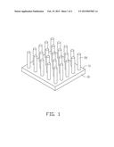
[0009] FIG. 1 illustrates a heat sink for dissipating heat generated by an electronic component and protecting the electronic component from electromagnetic interference (EMI).
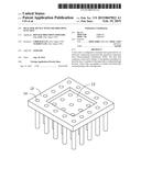
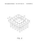
[0010] FIG. 2 illustrates the heat sink from another angle.
[0011] The heat sink can comprise a base 10 and a plurality of waveguides 20 extending out from the base 10. A receiving cutout 13 is defined in a lower surface 12 of the base 10. The electronic component is received in the receiving cutout 13. A plurality of through holes 14 is defined through the base 10.
[0012] Each waveguide 20 is a hollow tube made of metal, or other thermally conductive materials. One end of each waveguide 20 is open to communicate with a corresponding through hole 14 of the base 10. Another end of each waveguide 20 is closed. The base 10 and the waveguide 20 can be attached together or integrally formed.
[0013] During assembly, the heat sink can be mounted on the electronic component, with the electronic component received in the receiving cutout 13. Thus, the heat sink is capable of not only protecting the electronic component received in the receiving cutout 13 from electromagnetic waves generated by other electronic components, but also preventing electromagnetic waves generated by the electronic component received in the receiving cutout 13 from interfering with the other electronic components. The heat sink is also capable of effectively dissipating heat generated by the electronic component received in the receiving cutout 13.
[0014] The embodiments shown and described above are only examples. Even though numerous characteristics and advantages of the present technology have been set forth in the foregoing description, together with details of the structure and function of the present disclosure, the disclosure is illustrative only, and changes may be made in the detail, including in matters of shape, size and arrangement of the parts within the principles of the present disclosure up to, and including, the full extent established by the broad general meaning of the terms used in the claims.
User Contributions:
Comment about this patent or add new information about this topic:
Images included with this patent application:
 |  |
 |
| Similar patent applications: | |
| Date | Title |
|---|---|
| 2015-03-19 | Substrate temperature regulating device and substrate processing apparatus using the same |
| 2015-02-19 | Heating device structure |
| 2015-03-19 | Surface treatment for corrosion resistance of aluminum |
| 2015-03-19 | Heat exchange element and air conditioner |
| 2015-03-19 | Multi-level redundant cooling method for continuous cooling of an electronic system(s) |
| New patent applications from these inventors: | |
| Date | Title |
|---|---|
| 2015-04-16 | Casing for receiving hard disk drive |
| 2015-01-29 | Supporting apparatus for electrostatic gun |
| 2014-12-25 | Waveguide tube with adjustability between outputs |
| 2014-06-26 | Electromagnetic interference shield and electronic device using the same |
| Top Inventors for class "Heat exchange" | |
| Rank | Inventor's name |
|---|---|
| 1 | Levi A. Campbell |
| 2 | Chun-Chi Chen |
| 3 | Tai-Her Yang |
| 4 | Robert E. Simons |
| 5 | Richard C. Chu |