Patent application title: POLARIZER STRUCTURE
Inventors:
Chih-Chung Lin (Taipei City, TW)
Chih-Chung Lin (Taipei City, TW)
IPC8 Class: AG02F11333FI
USPC Class:
349 12
Class name: Liquid crystal cells, elements and systems liquid crystal system liquid crystal writing tablet
Publication date: 2014-06-19
Patent application number: 20140168532
Abstract:
A polarizer structure includes a transparent substrate, a sensor, a
polarizing plate and a first insulating adhesive layer. The sensor is
coated on one side of the transparent substrate, and the first insulating
adhesive layer is arranged between the sensor and the polarizing plate to
bond them together. The polarizer structure is configured for arrangement
on a liquid crystal display (LCD) unit to make the latter a touch screen,
on which a user can input and do other operations by touching the
polarizer structure. In this manner, a touch screen can be manufactured
with reduced cost and increased good yield rate.Claims:
1. A polarizer structure, comprising a transparent substrate defining a
first side and an opposite second side; a sensor coated on the second
side of the transparent substrate; a polarizing plate defining a third
side and an opposite fourth side, and correspondingly attached at the
third side to the sensor; and a first insulating adhesive layer arranged
between the sensor and the polarizing plate.
2. The polarizer structure as claimed in claim 1, wherein the polarizer structure is configured for applying to a liquid crystal display (LCD) unit by attaching the fourth side of the polarizing plate to the liquid crystal display (LCD) unit.
3. The polarizer structure as claimed in claim 2, wherein the LCD unit includes a first substrate, a second substrate, and a liquid crystal layer sandwiched between the first and the second substrate.
4. The polarizer structure as claimed in claim 2, wherein the fourth side of the polarizing plate is attached to the LCD unit via a second insulating adhesive layer arranged between the polarizing plate and the LCD unit.
5. The polarizer structure as claimed in claim 1, wherein the sensor is a thin film formed of a material selected from the group consisting of indium tin oxide (ITO), antimony tin oxide (ATO) and indium zinc oxide (IZO).
6. The polarizer structure as claimed in claim 4, wherein the first and the second insulating adhesive layer are selected from the group consisting of an optical clear adhesive (OCA) and an optical clear resin (OCR).
7. The polarizer structure as claimed in claim 1, wherein the transparent substrate is made of a material selected from the group consisting of glass, polyethylene terephthalate (PET), polycarbonate (PC), polyethylene (PE), polyvinylchloride (PVC), polypropylene (PP), polystyrene (PS), polymethylmethacrylate (PMMA), and cycle olefin copolymer (COC).
8. The polarizer structure as claimed in claim 1, further comprising a flexible circuit board having a portion attached to an edge of the sensor via a conductive adhesive layer applied between the flexible circuit board and the sensor.
9. The polarizer structure as claimed in claim 8, wherein the first insulating adhesive layer covers the sensor and the portion of the flexible circuit board attached to the sensor.
10. The polarizer structure as claimed in claim 3, wherein the LCD unit further includes a lower polarizing plate located on one side of the second substrate opposite to the liquid crystal layer.
Description:
[0001] This application claims the priority benefit of Taiwan patent
application number 101145212 filed on Dec. 19, 2012.
FIELD OF THE INVENTION
[0002] The present invention relates to a polarizer, and more particularly to a polarizer structure that can be correspondingly arranged on a liquid crystal display (LCD) unit to make the latter a touch screen that can be manufactured with reduced cost and increased good yield rate.
BACKGROUND OF THE INVENTION
[0003] Many electronic products, such as the currently available personal digital assistant (PDAs), palm-sized personal computers (PCs) and information appliances, usually have a display screen with a touch panel. Functional images and texts are shown on the display screen via the touch panel, and a user may select any desired image or text by touching the touch panel with a conductive object, such as a fingertip or a touch pen, to complete input and other operations. Therefore, a touch screen plays a very important role in enabling highly humanized manipulation of electronic products.
[0004] Most of the current touch panel technologies are developed and designed to achieve the object of directly integrating a touch panel into a display screen. Presently, there are two major types of such technologies, namely, in-cell touch technology and on-cell touch technology. In the on-cell touch technology, the x-axis sensors and the y-axis sensors in the projected-capacitive touch technology are produced on a back of the color filter (CF) of a display screen to thereby integrate with the CF.
[0005] In the in-cell touch technology, the x-axis sensors and the y-axis sensors are integrated into a liquid crystal display (LCD) cell. In other words, with the in-cell touch technology, the touch sensor elements are integrated into a glass substrate of the display panel, so that the display panel itself functions like a touch panel without the need of having another separate touch panel laminated or assembled thereto.
[0006] However, either the in-cell touch technology or the on-cell touch technology includes the manufacturing process of providing a plurality of sensors, i.e. the x-axis sensors and the y-axis sensors, in an upper or a lower glass substrate of the LCD display panel. Therefore, the manufacturing process not only requires increased cost, but also need multiple processing masks because the x-axis sensors and the y-axis sensors must be bridged in the manufacturing process. As a result, increased manufacturing procedures are involved that in turn causes lowered good yield rate and increased manufacturing cost. Therefore, it is desirable to further improve the conventional touch display devices.
[0007] In brief, the conventional ways for manufacturing touch screens have the following disadvantages: (1) having lowered good yield rate, and (2) increasing the manufacturing cost.
[0008] It is therefore tried by the inventor to develop a polarizer structure for overcoming the problems in manufacturing the conventional touch screens.
SUMMARY OF THE INVENTION
[0009] A primary object of the present invention is to provide a polarizer structure that enables the manufacture of a touch screen with reduced cost and increased good yield rate.
[0010] To achieve the above and other objects, the polarizer structure according to the present invention includes a transparent substrate, a sensor, a polarizing plate and a first insulating adhesive layer. The transparent substrate defines a first side and an opposite second side, and the sensor is coated on the second side of the transparent substrate. The polarizing plate defines a third side and an opposite fourth side, and is attached at the third side to the sensor via the first insulating adhesive layer provided between the sensor and the polarizing plate. The polarizer structure can be correspondingly arranged on a liquid crystal display (LCD) unit to make the latter a touch screen, on which a user can input and make other operations by touching the polarizer structure. In this manner, a touch screen can be manufactured with reduced cost and increased good yield rate.
BRIEF DESCRIPTION OF THE DRAWINGS
[0011] The structure and the technical means adopted by the present invention to achieve the above and other objects can be best understood by referring to the following detailed description of the preferred embodiments and the accompanying drawings, wherein
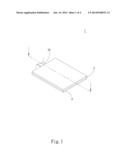
[0012] FIG. 1 is an assembled perspective view of a polarizer structure according to a preferred embodiment of the present invention;
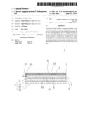
[0013] FIG. 2 is a sectional view of FIG. 1;
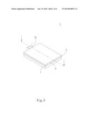
[0014] FIG. 3 is an assembled perspective view showing an application of the polarizer structure according to the preferred embodiment of the present invention to a liquid crystal display (LCD) unit; and
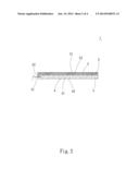
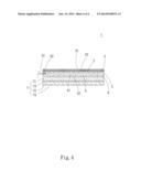
[0015] FIG. 4 is a sectional view of FIG. 3.
DETAILED DESCRIPTION OF THE PREFERRED EMBODIMENTS
[0016] The present invention will now be described with a preferred embodiment thereof and with reference to the accompanying drawings.
[0017] Please refer to FIGS. 1 and 2 that are assembled perspective and sectional views, respectively, of a polarizer structure 1 according to a preferred embodiment of the present invention. As shown, the polarizer structure 1 includes a transparent substrate 2, a sensor 3, a polarizing plate 4, and a first insulating adhesive layer 5. While the illustrated preferred embodiment is described with the transparent substrate 2 being made of a polyethylene terephthalate (PET) material, it is understood the transparent substrate 2 can be otherwise made of glass, polycarbonate (PC), polyethylene (PE), polyvinylchloride (PVC), polypropylene (PP), polystyrene (PS), polymethylmethacrylate (PMMA), or cycle olefin copolymer (COC).
[0018] The transparent substrate 2 defines a first side 21 and an opposite second side 22. The sensor 3 is provided on the second side 22 of the transparent substrate 2. The sensor 3 can be a thin film of indium tin oxide (ITO), antimony tin oxide (ATO) or indium zinc oxide (IZO). In the illustrated preferred embodiment, the sensor 3 is formed on the second side 22 of the transparent substrate 2 by means of sputtering deposition. However, in practical implementation of the present invention, the sensor 3 can be otherwise formed on the second side 22 of the transparent substrate 2 by gel coating, electroplating or vapor deposition. A flexible circuit board 31 is attached to an edge of the sensor 3 via a conductive adhesive layer 32 applied between the flexible circuit board 31 and the sensor 3. In the illustrated preferred embodiment, the conductive adhesive layer 32 is an anisotropic conductive film (ACF). In other words, the flexible circuit board 31 has an end bonded to one side of the conductive adhesive layer 32 opposite to the sensor 3, so that the flexible circuit board 31 is electrically connected at the end to the sensor 3 via the conductive adhesive layer 32.
[0019] The polarizing plate 4 defines a third side 41 and an opposite fourth side 42. The third side 41 of the polarizing plate 4 is correspondingly attached to the sensor 3 and the flexible circuit board 31 via the first insulating adhesive layer 5 provided between the third side 41 of the polarizing plate 4 and the sensor 3 and the flexible circuit board 31. In the present invention, the first insulating adhesive layer 5 can be an optical clear adhesive (OCA) or an optical clear resin (OCR).
[0020] Please refer to FIGS. 3 and 4 that are assembled perspective and sectional views, respectively, showing an application of the polarizer structure 1 according to the preferred embodiment of the present invention to a liquid crystal display (LCD) unit 7. As shown, the LCD unit 7 includes a first substrate 71, a second substrate 72, a liquid crystal layer 73 and a lower polarizing plate 74. The liquid crystal layer 73 is sandwiched between the first substrate 71 and the second substrate 72, and the lower polarizing plate 74 is located on one side of the second substrate 72 opposite to the liquid crystal layer 73. The LCD unit 7 is attached to the fourth side 42 of the polarizing plate 4 via a second insulating adhesive layer 6 applied between the first substrate 71 and the polarizing plate 4. Again, the second insulating adhesive layer 6 can be an optical clear adhesive (OCA) or an optical clear resin (OCR). By attaching the polarizer structure 1 having the sensor 3 and the polarizing plate 4 to the LCD unit 7, the LCD unit 7 can now function like a touch screen that allows a user to control input and other operations thereon by touching the polarizer structure 1. With the present invention, the LCD unit 7 functioning like a touch screen can be manufactured with reduced cost and increased good yield rate.
[0021] In brief, compared to the prior art, the present invention has the following advantages: (1) enabling increased good yield rate of touch screens; and (2) enabling reduced manufacturing cost of touch screens.
[0022] The present invention has been described with a preferred embodiment thereof and it is understood that many changes and modifications in the described embodiment can be carried out without departing from the scope and the spirit of the invention that is intended to be limited only by the appended claims.
User Contributions:
Comment about this patent or add new information about this topic:
Images included with this patent application:
 |  |
 |  |
 |
| Similar patent applications: | |
| Date | Title |
|---|---|
| 2014-02-27 | Polarizer resistive touch screen |
| 2012-04-26 | Pixel array structure |
| 2012-08-30 | Pixel array structure |
| 2010-01-14 | Spacer structure |
| 2011-05-19 | Electric circuit structure |
| New patent applications in this class: | |
| Date | Title |
|---|---|
| 2019-05-16 | Display device and electronic apparatus |
| 2019-05-16 | In-cell touch-sensitive liquid crystal display device |
| 2018-01-25 | Liquid crystal display device having touch and three-dimensional display functions and method for manufacturing the same |
| 2017-08-17 | Thin film transistor array substrate, manufacturing method thereof and touch display panel |
| 2017-08-17 | Liquid crystal display device |
| New patent applications from these inventors: | |
| Date | Title |
|---|---|
| 2016-06-30 | Touch panel with fingerprint recognition |
| 2016-06-30 | Touch panel capable of identifying fingerprint |
| 2016-05-26 | Touch panel with fingerprint identification function |
| 2016-05-26 | Touch panel structure |
| 2016-03-03 | Wearable electronic device |
| Top Inventors for class "Liquid crystal cells, elements and systems" | |
| Rank | Inventor's name |
|---|---|
| 1 | Shunpei Yamazaki |
| 2 | Hajime Kimura |
| 3 | Jae-Jin Lyu |
| 4 | Dong-Gyu Kim |
| 5 | Shunpei Yamazaki |