Patent application title: DC-DC Converter, Timing Signal Generating Circuit, and Operating Method Thereof
Inventors:
Wei-Ling Chen (Zhubei City, TW)
Assignees:
UPI SEMICONDUCTOR CORP.
IPC8 Class: AH02M3158FI
USPC Class:
323271
Class name: Using a three or more terminal semiconductive device as the final control device including plural final control devices switched (e.g., on-off control)
Publication date: 2014-06-19
Patent application number: 20140167716
Abstract:
A DC-DC converter including an output stage, a feedback loop, a
pulse-width modulation (PWM) generating circuit, and a driving circuit is
disclosed. The output stage is coupled to an input voltage and an output
inductor to provide an output voltage. The feedback loop is coupled to
the output inductor and receives the output voltage to generate a control
signal. The PWM generating circuit is coupled to the feedback loop and
receives the control signal. The PWM generating circuit also includes a
timing signal generating unit which makes the PWM generating circuit to
generate a PWM signal according to a correction voltage. The correction
voltage is reacted in the output voltage and a first current source
related to the input voltage.
The driving circuit is coupled to the output stage and the PWM generating
circuit and receives the PWM signal to control the operation of the
output stage.Claims:
1. A DC-DC converter, coupled to an input voltage and an output inductor,
the DC-DC converter comprising: an output stage, coupled to the input
voltage and the output inductor and providing an output voltage; a
feedback loop, coupled to the output inductor and receiving the output
voltage to generate a control signal; a pulse-width modulation (PWM)
generating circuit, coupled to the feedback loop and receiving the
control signal, wherein the PWM generating circuit comprises a timing
signal generating unit making the PWM generating circuit to generate a
PWM signal according to a correction voltage, and the correction voltage
responds the output voltage and a first current source related to the
input voltage; and a driving circuit, coupled to the output stage and the
PWM generating circuit and receiving the PWM signal to control the
operation of the output stage.
2. The DC-DC converter of claim 1, wherein the timing signal generating unit comprises a correction resistor, the correction voltage equals to the output voltage minus the product of the first current source and the correction resistor.
3. The DC-DC converter of claim 1, wherein the timing signal generating unit comprises a correction resistor and a metal-oxide-semiconductor field-effect transistor (MOSFET) buffer, the correction voltage equals to the output voltage plus a threshold voltage of the MOSFET buffer and then minus the product of the first current source and the correction resistor.
4. A timing signal generating circuit, applied in a PWM generating circuit of a DC-DC converter, the DC-DC converter coupling to an input voltage and providing an output voltage, the timing signal generating circuit comprising: a timing signal generating unit, comprising: a timing signal circuit, for receiving a PWM control signal and generating a time control signal according to the PWM control signal and a first current source related to the input voltage; a correction circuit, comprising the first current source and a correction resistor and responding the input voltage and the output voltage to provide a correction voltage; and a comparator, coupled to the timing signal circuit and the correction circuit, for making the PWM generating circuit to generate a PWM signal.
5. The timing signal generating circuit of claim 4, wherein the correction circuit further comprises a buffer unit.
6. The timing signal generating circuit of claim 5, wherein the buffer unit is an operational amplifier buffer.
7. The timing signal generating circuit of claim 5, wherein the buffer unit is a MOSFET buffer.
8. An operating method for a DC-DC converter, the DC-DC converter comprising an output stage, a feedback loop, a PWM generating circuit, and a driving circuit, the output stage being coupled to an input voltage and an output inductor, the feedback loop is coupled to the output inductor, the operating method comprising steps of: using the output stage to provide an output voltage; using the feedback loop to receive the output voltage and generate a control signal; using the PWM generating circuit to receive the control signal and generate a PWM signal according to a correction voltage, wherein the correction voltage responds the output voltage and a first current source related to the input voltage; and using the driving circuit to receive the PWM signal to control the operation of the output stage.
9. The operating method of claim 8, wherein the PWM generating circuit comprises a correction resistor, the correction voltage equals to the output voltage minus the product of the first current source and the correction resistor.
10. The operating method of claim 8, wherein the PWM generating circuit comprises a correction resistor and a MOSFET buffer, the correction voltage equals to the output voltage plus a threshold voltage of the MOSFET buffer and then minus the product of the first current source and the correction resistor.
11. An operating method for a timing signal generating circuit applied in a PWM generating circuit of a DC-DC converter, the DC-DC converter coupling to an input voltage and providing an output voltage, the timing signal generating circuit comprising a timing signal circuit, a correction circuit, and a comparator, the operating method comprising steps of: using the timing signal circuit to generate a time control signal according to the PWM control signal and a first current source related to the input voltage; using the correction circuit to respond the input voltage and the output voltage to provide a correction voltage; and using the comparator to receive the time control signal and the correction voltage and make the PWM generating circuit to generate a PWM signal.
12. The operating method of claim 11, further comprising a step of providing an operational amplifier buffer as a buffer unit in the correction circuit.
13. The operating method of claim 11, further comprising a step of providing an MOSFET buffer as a buffer unit in the correction circuit.
Description:
BACKGROUND OF THE INVENTION
[0001] 1. Field of the invention
[0002] The invention relates to a DC-DC converter; in particular, to a DC-DC converter, a timing signal generating circuit, and operating methods thereof.
[0003] 2. Description of the prior art
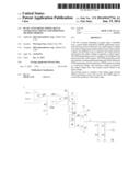
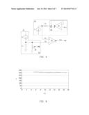
[0004] Please refer to FIG. 1. FIG. 1 illustrates a functional block diagram of a one-shot timing generator of a conventional DC-DC converter. As shown in FIG. 1, the one-shot timing generator TG is used to output a pulse signal ONT_OUT to control a gate control unit and further control a gate driver to output a switch conducting signal to an output stage. However, in practical applications, the pulse width of the pulse signal ONT_OUT is not always equal to the pulse width of the switch conducting signal due to non-ideal factors such as signal propagation delay, driver delay, or other delay caused by parasitic capacitances. The on-time (Ton) will be affected by these non-ideal factors to generate an error time, and the proportion of the error time under different input voltages will be different; therefore, it will cause an error generated in the system operation frequency.
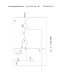
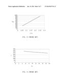
[0005] Please refer to FIG. 2. FIG. 2 illustrates a curve diagram of the on-time (Ton) varied with the reciprocal of the input voltage (VIN). As shown in FIG. 2, the intercept 52.041 of the curve y=3532.8×+52.041 with the vertical axis y is the error time of the on-time (Ton) under the non-ideal condition. As shown in FIG. 3, the system operation frequency (f) will be affected by this error time, and the system operation frequency (f) under different input voltages (VN) will be also different. Especially, when the input voltage is at high-level, the system operation frequency will become lower, and the normal system operation will be affected.
[0006] Therefore, the invention provides a DC-DC converter, a timing signal generating circuit, and operating methods thereof to solve the above-mentioned problems occurred in the prior arts.
SUMMARY OF THE INVENTION
[0007] A scope of the invention is to provide a DC-DC converter. In a preferred embodiment, the DC-DC converter is coupled to an input voltage and an output inductor. The DC-DC converter includes an output stage, a feedback loop, a pulse-width modulation (PWM) generating circuit, and a driving circuit. The output stage is coupled to the input voltage and the output inductor to provide an output voltage. The feedback loop is coupled to the output inductor and receives the output voltage to generate a control signal. The PWM generating circuit is coupled to the feedback loop and receives the control signal. The PWM generating circuit includes a timing signal generating unit making the PWM generating circuit to generate a PWM signal according to a correction voltage. The correction voltage responds the output voltage and a first current source related to the input voltage. The driving circuit is coupled to the output stage and the PWM generating circuit and receives the PWM signal to control the operation of the output stage.
[0008] Another scope of the invention is to provide a timing signal generating circuit. In a preferred embodiment, the timing signal generating circuit is applied in a PWM generating circuit of a DC-DC converter. The DC-DC converter is coupled to an input voltage to provide an output voltage. The timing signal generating circuit includes a timing signal generating unit. The timing signal generating unit includes a timing signal circuit, a correction circuit, and a comparator. The timing signal circuit is used for receiving a PWM control signal and generating a time control signal according to the PWM control signal and a first current source related to the input voltage. The correction circuit includes the first current source and a correction resistor and responds the input voltage and the output voltage to provide a correction voltage. The comparator is coupled to the timing signal circuit and the correction circuit and makes the PWM generating circuit to generate a PWM signal.
[0009] Another scope of the invention is to provide a DC-DC converter operating method. In a preferred embodiment, the DC-DC converter operating method is used to operate a DC-DC converter. The DC-DC converter includes an output stage, a feedback loop, a PWM generating circuit, and a driving circuit. The output stage is coupled to the input voltage and the output inductor. The feedback loop is coupled to the output inductor. The DC-DC converter operating method includes steps of: using the output stage to provide an output voltage; using the feedback loop to receive the output voltage and generate a control signal; using the PWM generating circuit to receive the control signal and generate a PWM signal according to a correction voltage, wherein the correction voltage responds the output voltage and a first current source related to the input voltage; and using the driving circuit to receive the PWM signal to control the operation of the output stage.
[0010] Another scope of the invention is to provide a timing signal generating circuit operating method. In a preferred embodiment, the timing signal generating circuit operating method is applied in a PWM generating circuit of a DC-DC converter.
[0011] The DC-DC converter is coupled to an input voltage and provides an output voltage. The timing signal generating circuit includes a timing signal circuit, a correction circuit, and a comparator. The timing signal generating circuit operating method includes steps of: using the timing signal circuit to generate a time control signal according to the PWM control signal and a first current source related to the input voltage; using the correction circuit to respond the input voltage and the output voltage to provide a correction voltage; and using the comparator to receive the time control signal and the correction voltage and make the PWM generating circuit to generate a PWM signal.
[0012] Compared to the prior arts, the DC-DC converter, the timing signal generating circuit, and the operating methods thereof disclosed by the invention can minus the error time varied with the input voltage from the on-time to effectively reduce the non-ideal error time effect on the system operation frequency caused by the signal propagation delay, driver delay, or other delay caused by parasitic capacitances.
[0013] Therefore, constant on-time and operation frequency can be maintained instead of being varied with the input voltage to enhance the system static stability and improve the electro-magnetic interference phenomenon.
[0014] The advantage and spirit of the invention may be understood by the following detailed descriptions together with the appended drawings.
[0015] BRIEF DESCRIPTION OF THE APPENDED DRAWINGS
[0016] FIG. 1 illustrates a functional block diagram of a one-shot timing generator of a conventional DC-DC converter.
[0017] FIG. 2 illustrates a curve diagram of the on-time (Ton) varied with the reciprocal of the input voltage (VIN).
[0018] FIG. 3 illustrates different system operation frequencies under different input voltages.
[0019] FIG. 4 illustrates a functional block diagram of the DC-DC converter in an embodiment of the invention.
[0020] FIG. 5 illustrates a functional block diagram of the timing signal generating unit in an embodiment of the invention.
[0021] FIG. 6 illustrates a schematic diagram of the corrected operation frequency not varied with the input voltage.
[0022] FIG. 7 illustrates a functional block diagram of the timing signal generating circuit in another embodiment of the invention.
[0023] FIG. 8 illustrates a flowchart of the DC-DC converter operating method in another embodiment of the invention.
[0024] FIG. 9 illustrates a flowchart of the timing signal generating circuit operating method in another embodiment of the invention.
DETAILED DESCRIPTION OF THE INVENTION
[0025] A preferred embodiment of the invention is a DC-DC converter. In fact, the DC-DC converter of the invention has constant on-time, and can be applied in power conversion circuit structures of the AC-DC converter or the DC-AC converter. It should be noticed that "coupled" in the invention can be various types of directly coupled, indirectly coupled, or electrically connected without limiting their connection relationship.
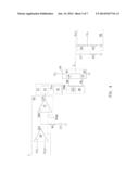
[0026] Please refer to FIG. 4. The DC-DC converter 1 includes an error amplifier 10, a comparator 12, a timing signal generating unit 14, a gate control unit 16, a gate driver 18, an output stage 19, an output inductor L, a first voltage-dividing resistor R1, a second voltage-dividing resistor R2, resistors R3˜R4, and capacitors C1˜C2. The output stage 19 includes a first transistor Q1 and a second transistor Q2. A feedback loop FB includes the first voltage-dividing resistor R1, the second voltage-dividing resistor R2, the error amplifier 10, and the comparator 12. A pulse-width modulation (PWM) generating circuit 13 includes the timing signal generating unit 14 and the gate control unit 16. A driving circuit DR includes the gate driver 18.
[0027] The error amplifier 10 is coupled to the comparator 12; the resistor R4 is coupled between the error amplifier 10 and the comparator 12; the capacitor C2 is coupled between the resistor R4 and the ground terminal; the timing signal generating unit 14 is coupled between the comparator 12 and the gate control unit 16; the gate control unit 16 is coupled between the timing signal generating unit 14 and the gate driver 18; the gate driver 18 is coupled to the gates of the first transistor Q1 and the second transistor Q2 respectively; the first transistor Q1 and the second transistor Q2 are coupled in series between an input voltage VIN and the ground terminal; one end of the output inductor L is coupled between the first transistor Q1 and the second transistor Q2, and the other end of the output inductor L is coupled to the output voltage VOUT; the capacitor C1 is coupled between the output inductor L and the output voltage VOUT; the resistor R3 is coupled between the capacitor C1 and the ground terminal; the first voltage-dividing resistor R1 is coupled between the output inductor L and the output voltage VOUT; the second voltage-dividing resistor R2 is coupled between the first voltage-dividing resistor R1 and the ground terminal
[0028] A negative input terminal - of the error amplifier 10 is coupled between the first voltage-dividing resistor R1 and the second voltage-dividing resistor R2 to receive a feedback voltage Vfb; a positive input terminal + of the error amplifier 10 receives a reference voltage Vref; an output terminal 10A of the error amplifier 10 outputs an error amplifying signal ERR. A positive input terminal + of the comparator 12 receives the error amplifying signal ERR; a negative input terminal - of the comparator 12 receives a ramp signal Ramp; an output terminal 12A of the comparator 12 outputs a control signal to the timing signal generating unit 14.
[0029] The timing signal generating unit 14 is corrected according to the correction voltage to output a constant on-time signal Ton to the gate control unit 16. The gate control unit 16 outputs a pulse-width modulation signal PWM to the gate driver 18 according to the on-time signal Ton. The gate driver 18 controls the operation of the output stage 19 according to the pulse-width modulation signal PWM to selectively output switch conducting signals DH and DL to the gates of the first transistor Q1 and the second transistor Q2 to control the first transistor Q1 and the second transistor Q2 switched on or off
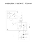
[0030] Next, the timing signal generating unit applied in the PWM generating circuit of the DC-DC converter will be introduced in detail as follows. As shown in FIG. 5, the timing signal generating unit 14 includes a timing signal circuit 5A, a correction circuit 5B, and a first comparator 50. In this embodiment, the timing signal circuit 5A includes a second current source I2, a capacitor Ci, and a switch SW; the correction circuit 5B includes a first current source I1, a correction resistor Ri, and an operational amplifier 52. In fact, the connecting way of the operational amplifier 52 can form an operational amplifier buffer OB as a buffer unit in the correction circuit 5B.
[0031] The capacitor Ci is coupled between the second current source I2 and the ground terminal; a positive input terminal + of the first comparator 50 is coupled between the correction resistor Ri and the first current source I1, and a negative input terminal - of the first comparator 50 is coupled among the second current source I2, the capacitor Ci, and the switch SW; the first current source I1 is coupled between the correction resistor Ri and the ground terminal; the correction resistor Ri is coupled between the operational amplifier 52 and the first current source I1; a positive input terminal +of the operational amplifier 52 is coupled to the output voltage VOUT, and a negative input terminal - of the operational amplifier 52 is coupled between an output terminal K of the operational amplifier 52 and the correction resistor Ri.
[0032] It should be noticed that the first current source I1 and the second current source I2 are functions of the input voltage VIN respectively, that is to say, the currents of the first current source I1 and the second current source I2 will be varied with the changing of the input voltage VIN.
[0033] The timing signal circuit 5A receives the pulse-width modulation signal PWM and generates a time control signal Vp according to the pulse-width modulation signal PWM and the second current source I2 related to the input voltage VIN.
[0034] In the correction circuit 5B, the voltage VR between the output terminal K of the operational amplifier 52 and the correction resistor Ri is approximately near the output voltage VOUT, and the voltage across the correction resistor Ri equals to the product of the first current source I1 and the correction resistor Ri. Therefore, the correction voltage Vm that the correction circuit 5B provides to the first comparator 50 is equal to the output voltage VOUT minus the product of the first current source I1 and the correction resistor Ri. That is to say, the correction voltage Vm=the output voltage VOUT-(the first current source I1*the correction resistor Ri). Since the first current source I1 is a function of the input voltage VIN, the correction voltage Vm provided by the correction circuit 5B is a function of the input voltage VIN and the output voltage VOUT to respond the input voltage VIN and the output voltage VOUT at the same time.
[0035] When the positive input terminal + of the first comparator 50 receives the correction voltage Vm from the correction circuit 5B and the negative input terminal - of the first comparator 50 receives the time control signal Vp from the timing signal circuit 5A, the first comparator 50 compares the time control signal Vp with the correction voltage Vm to generate the on-time signal Ton including the corrected on-time and output the on-time signal Ton through the output terminal J. It should be noticed that the corrected on-time equals to [the capacitor Ci*(the output voltage VOUT-the first current source I1*the correction resistor Ri)]/the second current source I2, that is to say, the corrected on-time is equal to the uncorrected on-time minus the error time. Therefore, after the on-time is corrected, the effect of the error time on the on-time can be effectively reduced.
[0036] The corrected result is shown in FIG. 6. As shown in FIG. 6, the corrected operation frequency will be stable without being varied with the different input voltages VN. It should be noticed that the first current source I1 becomes larger with the increasing of the input voltages VN. Therefore, when the input voltages VIN becomes larger, the on-time minus larger error time, namely the degree that the on-time is corrected also becomes larger.
[0037] Please refer to FIG. 7. FIG. 7 illustrates a functional block diagram of the timing signal generating circuit in another embodiment of the invention. As shown in FIG. 7, the timing signal generating circuit 7 includes a timing signal circuit 7A, a correction circuit 7B, and a first comparator 70. In this embodiment, the timing signal circuit 7A includes a second current source I2, a capacitor Ci, and a switch SW; the correction circuit 7B includes a first current source I1, a correction resistor Ri, and a buffer unit MB. The buffer unit MB includes a third current source I3, a second bias current source Ib2, a second transistor MP2, a first bias current source Ib1, and a first transistor MP1.
[0038] The capacitor Ci is coupled between the second current source I2 and the ground terminal; a gate of the first transistor MP1 is coupled between the second current source I2 and the capacitor Ci, and a source and a drain of the first transistor MP1 are coupled to the first bias current source Ib1 and the ground terminal respectively; a positive input terminal + of the first comparator 70 is coupled between the correction resistor Ri and the first current source I1, a negative input terminal - of the first comparator 70 is coupled between the first bias current source Ib1 and the first transistor MP1; the first current source I1 is coupled between the correction resistor Ri and the ground terminal; one end of the correction resistor Ri is coupled to the first current source I1 and the positive input terminal + of the first comparator 70, and the other end of the correction resistor Ri is coupled to the second transistor MP2, the second bias current source Ib2, and the third current source I3; a gate of the second transistor MP2 is coupled to the output voltage VOUT, and a source and a drain of the second transistor MP2 are coupled to the ground terminal, the second bias current source Ib2, and the third current source 13 respectively.
[0039] It should be noticed that the first current source I1, the second current source I2, and the third current source 13 are functions of the input voltage VIN respectively; that is to say, the currents of the first current source I1, the second current source I2, and the third current source 13 are varied with the changing of the input voltage VIN.
[0040] In addition, the current value of the first current source I1 is equal to the current value of the third current source 13 to maintain the common mode level of the second transistor MP2.
[0041] The timing signal circuit 7A receives the pulse-width modulation signal PWM and generates a time control signal Vp to a gate of the first transistor MP1 according to the pulse-width modulation signal PWM and the second current source I2 related to the input voltage VIN. A voltage VB between the first bias current source Ib1 and the first transistor MP1 is equal to the sum of a threshold voltage Vth of the first transistor MP1 and the time control signal Vp. A correction voltage VA between the correction resistor Ri and the first current source I1 is equal to the output voltage VOUT plus the threshold voltage Vth of the second transistor MP2 and then minus the product of the first current source I1 and the correction resistor Ri. That is to say, the correction voltage VA=the output voltage VOUT +the threshold voltage Vth of the second transistor MP2-(the first current source I1*the correction resistor Ri). Since the first current source I1 is a function of the input voltage VN, the correction voltage VA provided by the correction circuit 5B is a function of the input voltage VIN and the output voltage VOUT to respond the input voltage VN and the output voltage VOUT at the same time.
[0042] When the positive input terminal + of the first comparator 70 receives the correction voltage VA and the negative input terminal - of the first comparator 70 receives the voltage VB, the first comparator 70 compares the voltage VB with the correction voltage VA to generate the on-time signal Ton including the corrected on-time and output the on-time signal Ton through the output terminal J.
[0043] In fact, the first transistor MP1 and the second transistor MP2 in the buffer unit MB of the correction circuit 7B can be MOSFETs, and the buffer unit MB can be MOSFET buffer, but not limited to this.
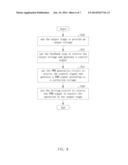
[0044] Another preferred embodiment of the invention is a DC-DC converter operating method. In this embodiment, the DC-DC converter operating method is used to operate a DC-DC converter having a constant on-time. The DC-DC converter includes an output stage, a feedback loop, a PWM generating circuit, and a driving circuit. The output stage is coupled to the input voltage and the output inductor. The feedback loop is coupled to the output inductor. Please refer to FIG. 8. FIG. 8 illustrates a flowchart of the DC-DC converter operating method in this embodiment.
[0045] As shown in FIG. 8, at first, in the step S10, the method uses the output stage to provide an output voltage. Then, in the step S12, the method uses the feedback loop to receive the output voltage and generate a control signal. Next, in the step S14, the method uses the PWM generating circuit to receive the control signal and generate a
[0046] PWM signal according to a correction voltage, wherein the correction voltage responds the output voltage and a first current source related to the input voltage. Afterwards, in the step S16, the method uses the driving circuit to receive the PWM signal to control the operation of the output stage.
[0047] It should be noticed that there are two ways for the method to perform the step S14 as follows. (1) If the timing signal generating unit of the PWM generating circuit includes a correction resistor, then the correction voltage used in the step S14 is equal to the output voltage minus the product of the first current source and the correction resistor. (2) If the timing signal generating unit of the PWM generating circuit includes a correction resistor and a MOSFET buffer, then the correction voltage used in the step S14 is equal to the output voltage plus the threshold voltage of the MOSFET buffer and then minus the product of the first current source and the correction resistor.
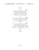
[0048] Another preferred embodiment of the invention is a timing signal generating circuit operating method. In this embodiment, the timing signal generating circuit operating method is applied in a PWM generating circuit of a DC-DC converter. The DC-DC converter is coupled to an input voltage and provides an output voltage. The timing signal generating circuit includes a timing signal circuit, a correction circuit, and a comparator. Please refer to FIG. 9. FIG. 9 illustrates a flowchart of the timing signal generating circuit operating method in this embodiment.
[0049] As shown in FIG. 9, at first, in the step S20, the method uses the timing signal circuit to generate a time control signal according to the PWM control signal and a first current source related to the input voltage. Then, in the step S22, the method uses the correction circuit to respond the input voltage and the output voltage to provide a correction voltage. Afterwards, in the step S24, the method uses the comparator to receive the time control signal and the correction voltage and make the PWM generating circuit to generate a PWM signal.
[0050] In practical applications, the method can provide an operational amplifier buffer or a MOSFET buffer as a buffer unit in the correction circuit, but not limited to this.
[0051] Compared to the prior arts, the DC-DC converter, the timing signal generating circuit, and the operating methods thereof disclosed by the invention can minus the error time varied with the input voltage from the on-time to effectively reduce the non-ideal error time effect on the system operation frequency caused by the signal propagation delay, driver delay, or other delay caused by parasitic capacitances. Therefore, constant on-time and operation frequency can be maintained instead of being varied with the input voltage to enhance the system static stability and improve the electro-magnetic interference phenomenon.
[0052] With the example and explanations above, the features and spirits of the invention will be hopefully well described. Those skilled in the art will readily observe that numerous modifications and alterations of the device may be made while retaining the teaching of the invention. Accordingly, the above disclosure should be construed as limited only by the metes and bounds of the appended claims.
User Contributions:
Comment about this patent or add new information about this topic:
Images included with this patent application:
 |  |
 |  |
 |  |
 |  |
| Similar patent applications: | |
| Date | Title |
|---|---|
| 2014-06-19 | Dc/dc converter with shunt circuitry |
| 2014-06-26 | Internal voltage generation circuits |
| 2014-06-26 | Feed-forward compensation for low-dropout voltage regulator |
| 2014-06-26 | Time sequence circuit for power supply unit |
| 2014-05-15 | Dc conversion circuit |
| New patent applications in this class: | |
| Date | Title |
|---|---|
| 2022-05-05 | Buck-boost converter |
| 2022-05-05 | Energy-absorbing circuits |
| 2022-05-05 | Control circuit and method for fuel-saving multi-state switch |
| 2019-05-16 | Voltage conversion device and method of deciding leakage inductance |
| 2019-05-16 | Frequency control circuit, control method and switching converter |
| New patent applications from these inventors: | |
| Date | Title |
|---|---|
| 2014-02-27 | Control circuit, time calculating unit, and operating method for control circuit |
| Top Inventors for class "Electricity: power supply or regulation systems" | |
| Rank | Inventor's name |
|---|---|
| 1 | Weihong Qiu |
| 2 | Benjamim Tang |
| 3 | Qian Ouyang |
| 4 | Ta-Yung Yang |
| 5 | John L. Melanson |