Patent application title: MULTIPLE QUANTUM WELL FOR ULTRAVIOLET LIGHT EMITTING DIODE AND A PRODUCTION METHOD THEREFOR
Inventors:
Byoung Gu Cho (Seoul, KR)
Jae-Sik Min (Seoul, KR)
Se-Hun Kwon (Busan, KR)
Assignees:
CHIP TECHNOLOGY CO., LTD
IPC8 Class: AH01L3306FI
USPC Class:
257 13
Class name: Thin active physical layer which is (1) an active potential well layer thin enough to establish discrete quantum energy levels or (2) an active barrier layer thin enough to permit quantum mechanical tunneling or (3) an active layer thin enough to permit carrier transmission with substantially no scattering (e.g., superlattice quantum well, or ballistic transport device) heterojunction incoherent light emitter
Publication date: 2014-06-12
Patent application number: 20140158981
Abstract:
A multiple quantum well structure for an ultraviolet light-emitting
diode, comprising: an Alx1Ga1-x1N barrier portion comprising an
AlN barrier atomic layer and a GaN barrier atomic layer, which are
alternately arranged; and an Alx2Ga1-x2N quantum well portion
formed on the Alx1Ga1-x1N barrier portion and comprising an AlN
well atomic layer and a GaN well atomic layer, which are alternately
arranged, wherein the Al composition ratio (x1) of the
Alx1Ga1-x2N barrier portion is 0-0.7, the Al composition ratio
(x2) of the Alx2Ga1-x2N quantum well portion is 0-0.7, the Al
composition ratio (x1) of the Alx1Ga1-x1N barrier portion is
greater than the Al composition ratio (x2) of the Alx2Ga1-x2N
quantum well portion, and the Alx1Ga1-x1N barrier portion and
the Alx2Ga1-x2N quantum well portion are alternately deposited
two or more times.Claims:
1. A multiple quantum well structure for an ultraviolet light-emitting
diode, comprising: an Alx1Ga1-x1N barrier portion comprising an
AlN barrier atomic layer and a GaN barrier atomic layer, which are
alternately arranged; and an Alx2Ga1-x2N quantum well portion
formed on the Alx1Ga1-x1N barrier portion and comprising an AlN
well atomic layer and a GaN well atomic layer, which are alternately
arranged, wherein the Al composition ratio (x1) of the
Alx1Ga1-x1N barrier portion is 0-0.7, the Al composition ratio
(x2) of the Alx2Ga1-x2N quantum well portion is 0-0.7, the Al
composition ratio (x1) of the Alx1Ga1-x1N barrier portion is
greater than the Al composition ratio (x2) of the Alx2Ga1-x2N
quantum well portion, and the Alx1Ga1-x1N barrier portion and
the Alx2Ga1-x2N quantum well portion are alternately deposited
two or more times.
2. The multiple quantum well structure of claim 1, wherein the Alx1Ga1-x1N barrier portion has a thickness of 3-10 nm.
3. The multiple quantum well structure of claim 1, wherein the Alx1Ga1-x1N barrier portion has a dislocation density of 10.sup.4-10.sup.6 ea/cm.sup.2.
4. The multiple quantum well structure of claim 1, wherein the Alx2Ga1-x2N quantum well portion has a thickness of 1-3 nm.
5. The multiple quantum well structure of claim 1, wherein the Alx2Ga1-x2N quantum well portion has a dislocation density of 10.sup.4-10.sup.6 ea/cm.sup.2.
6. The multiple quantum well structure of claim 1, wherein the number of the Alx2Ga1-x2N quantum well portions is 2-10.
7. A method for fabricating a multiple quantum well structure for an ultraviolet light-emitting diode, the method comprising the steps of: alternately depositing an AlN barrier atomic layer and a GaN barrier atomic layer to form an Alx1Ga1-x1N barrier portion; and alternately depositing an AlN well atomic layer and a GaN well atomic layer on the Alx1Ga1-x1N barrier portion to form an Alx2Ga1-x2N quantum well portion, wherein the Alx1Ga1-x1N barrier portion and the Alx2Ga1-x2N quantum well portion are formed such that the Al composition ratio (x1) of the Alx1Ga1-x1N barrier portion is 0-0.7, the Al composition ratio (x2) of the Alx2Ga1-x2N quantum well portion is 0-0.7, the Al composition ratio (x1) of the Alx1Ga1-x1N barrier portion is greater than the Al composition ratio (x2) of the Alx2Ga1-x2N quantum well portion, and the Alx1Ga1-x1N barrier portion and the Alx2Ga1-x2N quantum well portion are alternately deposited two or more times.
8. The method of claim 7, wherein the Alx1Ga1-x1N barrier portion is formed to have a thickness of 3-10 nm.
9. The method of claim 7, wherein the Alx1Ga1-x1N barrier portion has a dislocation density of 10.sup.4-10.sup.6 ea/cm.sup.2.
10. The method of claim 7, wherein the Alx2Ga1-x2N quantum well portion is formed to have a thickness of 1-3 nm.
11. The method of claim 7, wherein the Alx2Ga1-x2N quantum well portion has a dislocation density of 10.sup.4-10.sup.6 ea/cm.sup.2.
12. The method of claim 7, wherein the number of the Alx2Ga1-x2N quantum well portions deposited is 2-10.
Description:
BACKGROUND OF THE INVENTION
[0001] The present invention relates to a multiple quantum well structure for an ultraviolet light-emitting diode and a fabrication method thereof, and more particularly to a multiple quantum well structure for an ultraviolet light-emitting diode and a fabrication method thereof, in which the occurrence of dislocation can be effectively inhibited by alternately forming a high-quality barrier layer and a quantum well layer using atomic layer deposition (ALD) which can deposit layers at low temperature.
[0002] In recent years, a GaN-based light-emitting diode (LED) has received attention as the next-generation light-emitting device capable of maximizing energy saving. This GaN-based light-emitting diode emits light in the range from a visible light region to an ultraviolet light region.
[0003] In the prior art, a multiple quantum well structure for a light-emitting diode was fabricated by metal organic chemical vapor deposition (MOCVD).
[0004] However, in the case in which a light-emitting diode having a multiple quantum well structure was fabricated by metal organic chemical vapor deposition (MOCVD), the multiple quantum well structure was deposited at a temperature of 800° C. or higher, and thus dislocation caused by a difference in the coefficient of thermal expansion was widely generated. In addition, the light-emitting diode having this multiple quantum well structure had a very low light emission efficiency.
SUMMARY OF THE INVENTION
[0005] Accordingly, the present invention has been made in order to solve the problems occurring in the prior art, and it is an object of the present invention to provide a multiple quantum well structure for an ultraviolet light-emitting diode, in which the generation of dislocation can be effectively inhibited by alternately forming a high-quality barrier layer and a quantum well layer using atomic layer deposition (ALD) which can deposit layers at low temperature.
[0006] Another object of the present invention is to provide a method for fabricating the above-described multiple quantum well structure for an ultraviolet light-emitting diode, which can easily fabricate the multiple quantum well.
[0007] The objects to be achieved by the present invention are not limited to the above-mentioned objects, and other objects of the present invention will be clearly understood by those skilled in the art from the following description.
[0008] To achieve the above objects, in accordance with an embodiment of the present invention, there is provided a multiple quantum well structure for an ultraviolet light-emitting diode, comprising: an Alx1Ga1-x1N barrier portion comprising an AlN barrier atomic layer and a GaN barrier atomic layer, which are alternately arranged; and an Alx2Ga1-x2N quantum well portion formed on the Alx1Ga1-x1N barrier portion and comprising an AlN well atomic layer and a GaN well atomic layer, which are alternately arranged, wherein the Al composition ratio (x1) of the Alx1Ga1-x1N barrier portion is 0-0.7, the Al composition ratio (x2) of the Alx2Ga1-x2N quantum well portion is 0-0.7, the Al composition ratio (x1) of the Alx1Ga1-x1N barrier portion is greater than the Al composition ratio (x2) of the Alx2Ga1-x2N quantum well portion, and the Alx1Ga1-x1N barrier portion and the Alx2Ga1-x2N quantum well portion are alternately deposited two or more times.
[0009] In accordance with another embodiment of the present invention, there is provided a method for fabricating a multiple quantum well structure for an ultraviolet light-emitting diode, the method comprising the steps of: alternately depositing an AlN barrier atomic layer and a GaN barrier atomic layer to form an Alx1Ga1-x1N barrier portion; and alternately depositing an AlN well atomic layer and a GaN well atomic layer on the Alx1Ga1-x1N barrier portion to form an Alx2Ga1-x2N quantum well portion, wherein the Alx1Ga1-x1N barrier portion and the Alx2Ga1-x2N quantum well portion are formed such that the Al composition ratio (x1) of the Alx1Ga1-x1N barrier portion is 0-0.7, the Al composition ratio (x2) of the Alx2Ga1-x2N quantum well portion is 0-0.7, the Al composition ratio (x1) of the Alx1Ga1-x1N barrier portion is greater than the Al composition ratio (x2) of the Alx2Ga1-x2N quantum well portion, and the Alx1Ga1-x1N barrier portion and the Alx2Ga1-x2N quantum well portion are alternately deposited two or more times.
BRIEF DESCRIPTION OF THE DRAWINGS
[0010] FIG. 1 is a transmission electron micrograph of a multiple quantum well structure comprising an Alx1Ga1-x1N (0<x1<0.7) barrier portion and an Alx2Ga1-x2N (0≦x2<0.7, x2<x1) quantum well portions, fabricated by a method for fabricating a multiple quantum well structure for an ultraviolet light-emitting diode according to an embodiment of the present invention.
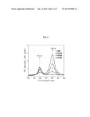
[0011] FIG. 2 is a graphic diagram showing the photoluminescence (PL) characteristics of multiple quantum well structures for ultraviolet light-emitting diodes, fabricated by depositing an Al0.36Ga0.64N (3.2 nm thick) barrier portion and a GaN (1.2 nm thick) quantum well portion according to embodiments of the present invention.
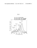
[0012] FIG. 3 is a graphic diagram showing the photoluminescence (PL) characteristics of multiple quantum well structures for ultraviolet light-emitting diodes, fabricated by alternately depositing an Al0.36Ga0.64N (3.2 nm thick) barrier portion and an AlxGa1-xN (1.2 nm thick, 0≦x2<0.2) quantum well portion six times.
DETAILED DESCRIPTION OF THE INVENTION
[0013] Hereinafter, preferred embodiments of the present invention will be described in detail with reference to the accompanying drawings.
[0014] FIG. 1 shows a multiple quantum well structure for an ultraviolet light-emitting diode according to an embodiment of the present invention. As shown in FIG. 1, an AlN barrier atomic layer and a GaN barrier atomic layer are alternately deposited to form an Alx1Ga1-x1N barrier portion.
[0015] Then, an AlN well atomic layer and a GaN well atomic layer are alternately deposited on the Alx1Ga1-x1N barrier portion to form an Alx2Ga1-x2N quantum well portion.
[0016] Herein, the Alx1Ga1-x1N barrier portion and Alx2Ga1-x2N quantum well portion of the multiple quantum well structure for the ultraviolet light-emitting diode according to the embodiment of the present invention are epitaxially grown on a substrate in the direction of crystal growth by supply of an aluminum source precursor and a gallium source precursor under high pressure at a temperature of 400° C. or lower using atomic layer deposition (ALD).
[0017] Meanwhile, the Alx1Ga1-x1N barrier portion and the Alx2Ga1-x2N quantum well portion are formed such that the Al composition ratio (x1) of the Alx1Ga1-x1N barrier portion is 0-0.7, the Al composition ratio (x2) of the Alx2Ga1-x2N quantum well portion is 0-0.7, and the Al composition ratio (x1) of the Alx1Ga1-x1N barrier portion is greater than the Al composition ratio (x2) of the Alx2Ga1-x2N quantum well portion. In addition, the Alx1Ga1-x1N barrier portion and the Alx2Ga1-x2N quantum well portion are alternately deposited two times or more.
[0018] If the Al composition ratio (x1) of the Alx1Ga1-x1N barrier portion or the Al composition ratio (x2) of the Alx2Ga1-x2N quantum well portion is greater than 0.7, the mismatch between the AlN material and the GaN material will increase, and thus surface defects can be formed.
[0019] Meanwhile, because the Alx1Ga1-x1N barrier portion or the Alx2Ga1-x2N quantum well portion is formed at a temperature of 400° C. using atomic layer deposition (ALD), the dislocation density of each of the portions can be controlled in the range of 104-106 ea/cm2.
[0020] Moreover, the Alx1Ga1-x1N barrier portion is formed to a thickness of 3-10 nm in order to inhibit the occurrence of direct tunneling. Preferably, the Alx1Ga1-x1N barrier portion is formed to a thickness between 3 nm and 5 nm.
[0021] Meanwhile, the Alx2Ga1-x2N quantum well portion is formed to a thickness between 1 nm and 3 nm. If the Alx2Ga1-x2N quantum well portion is formed to a thickness of less than 1 nm, intermixing of the Alx1Ga1-x1N barrier portion can occur, and if the thickness of the Alx2Ga1-x2N quantum well portion is more than 3 nm, the width of the band gap by the quantum effect will decrease, and thus the wavelength of light that is emitted from the multiple quantum well structure can increase. The Alx2Ga1-x2N quantum well portion is preferably formed to have a thickness between 1 nm and 2 nm.
[0022] Further, the wavelength of light that is emitted from a multiple quantum well structure for an ultraviolet light-emitting diode according to an embodiment of the present invention can be controlled by controlling the Al composition ratio (x2) of the Alx2Ga1-x2N quantum well portion. Specifically, when the Al composition ratio (x2) of the Alx2Ga1-x2N quantum well portion is 0, light having a wavelength of 360 nm will be emitted, and when the Al composition ratio (x2) of the Alx2Ga1-x2N quantum well portion is 0.7, light having a wavelength of 230 nm will be emitted. In addition, as the thickness of the Alx2Ga1-x2N quantum well portion decreases, the wavelength of light that is emitted from multiple quantum well structure decreases.
[0023] The number of Alx1Ga1-x1N barrier portions deposited and the number of Alx2Ga1-x2N quantum well portions deposited are each 2 to 10. If the number of the Alx1Ga1-x1N barrier portions and the Alx2Ga1-x2N quantum well portions increases, the volume of the active layer in the multiple quantum well structure will increase, and thus the light emission efficiency of the multiple quantum well structure will increase. However, the number of the Alx1Ga1-xN barrier portions and the Alx2Ga1-x2N quantum well portions excessively increases, the flow of electrons and holes between the Alx2Ga1-x2N quantum well portions will be difficult, and thus the light emission efficiency of the multiple quantum well structure can decrease. For this reason, the number of Alx1Ga1-x1N barrier portions deposited and the number of Alx2Ga1-x2N quantum well portions deposited are 10 or less. Preferably, the number of the Alx1Ga1-x1N barrier portions and the number of the Alx2Ga1-x2N quantum well portions are limited to 7 or less in view of the light emission efficiency.
[0024] FIG. 2 is a graphic diagram showing the photoluminescence (PL) characteristics of multiple quantum well structures for ultraviolet light-emitting diodes, fabricated by forming an Al0.36Ga0.64N (3.2 nm thick) barrier portion and a GaN (1.2 nm thick) quantum well portion according to embodiments of the present invention.
[0025] As shown in FIG. 2, when the number of quantum well portions is 7 or less, the photoluminescence intensity increases as the number of the quantum well portions increases. On the other hand, when the number of quantum well portions is more than 7, the photoluminescence intensity decreases as the number of the quantum well portions increases.
[0026] FIG. 3 is a graphic diagram showing the photoluminescence (PL) characteristics of multiple quantum well structures for ultraviolet light-emitting diodes, fabricated by alternately depositing an Al0.36Ga0.64N (3.2 nm thick) barrier portion and an AlxGa1-xN (1.2 nm thick, 0≦x2<0.2) quantum well portion six times. As shown in FIG. 3, as the Al composition ratio (x2) of the Alx2Ga1-x2N quantum well portion increase from 0 to 0.07 and 0.1, the wavelength of light emitted from the multiple quantum well structure decreases.
[0027] As described above, in the multiple quantum well structure for the ultraviolet light-emitting diode according to the embodiment of the present invention, the occurrence of dislocation can be effectively inhibited by alternately forming the high-quality barrier layer and the quantum well layer using atomic layer deposition (ALD) which can deposit layers at low temperature.
[0028] In addition, the method for fabricating the multiple quantum well structure for the ultraviolet light-emitting diode according to the embodiment of the present invention can easily fabricate the above-described multiple quantum well structure for the ultraviolet light-emitting diode.
[0029] Although the preferred embodiments of the present invention have been described for illustrative purposes, those skilled in the art will appreciate that various modifications, additions and substitutions are possible, without departing from the scope and spirit of the invention as disclosed in the accompanying claims.
User Contributions:
Comment about this patent or add new information about this topic:
| People who visited this patent also read: | |
| Patent application number | Title |
|---|---|
| 20150367058 | STACKED SORBENT ASSEMBLY |
| 20150367057 | RESERVE ZIRCONIUM PHOSPHATE MODULE FOR USE IN SORBENT DIALYSIS |
| 20150367056 | MODULAR DIALYSATE REGENERATION ASSEMBLY |
| 20150367055 | METHOD OF ZIRCONIUM PHOSPHATE RECHARGING |
| 20150367054 | ELECTROLYTE AND pH MONITORING FOR FLUID REMOVAL PROCESSES |
Images included with this patent application:
 |  |
| New patent applications in this class: | |
| Date | Title |
|---|---|
| 2022-05-05 | Quantum dot material, quantum dot light emitting device, display apparatus and manufacturing method |
| 2019-05-16 | Display device and manufacturing method of the same |
| 2019-05-16 | Polarization field assisted heterostructure design for efficient deep ultra-violet light emitting diodes |
| 2019-05-16 | Light emitting diode with high efficiency |
| 2019-05-16 | Patterned si substrate-based led epitaxial wafer and preparation method therefor |
| New patent applications from these inventors: | |
| Date | Title |
|---|---|
| 2014-10-23 | Light emitting diode package and method for manufacturing same |
| 2014-05-22 | Light diffusion of visible edge lines in a multi-dimensional modular display |
| 2014-03-20 | Multichip light emitting diode (led) and method of manufacture |
| 2013-07-04 | Semiconductor light emitting diode and method for manufacturing the same |
| Top Inventors for class "Active solid-state devices (e.g., transistors, solid-state diodes)" | |
| Rank | Inventor's name |
|---|---|
| 1 | Shunpei Yamazaki |
| 2 | Shunpei Yamazaki |
| 3 | Kangguo Cheng |
| 4 | Huilong Zhu |
| 5 | Chen-Hua Yu |