Patent application title: LIGHT EMITTING DIODE HAVING TWO SEPARATED SUBSTRATE PARTS CONNECTED TOGETHER BY ENCAPSULATION
Inventors:
Chao-Hsiung Chang (Hsinchu, TW)
Chao-Hsiung Chang (Hsinchu, TW)
Assignees:
ADVANCED OPTOELECTRONIC TECHNOLOGY, INC.
IPC8 Class: AH01L3352FI
USPC Class:
257 99
Class name: Active solid-state devices (e.g., transistors, solid-state diodes) incoherent light emitter structure with housing or contact structure
Publication date: 2014-04-03
Patent application number: 20140091354
Abstract:
A light emitting diode includes a substrate consisting two separated
parts with a gap therebetween. A first electrical connecting portion is
fixed to one of the two separated parts of the substrate and adjacent to
the gap. A second electrical connecting portion is fixed to the other one
of the two separated parts of the substrate and adjacent to the gap. An
LED chip is mounted on the substrate and electrically connected to the
first and second electrical connecting portions. An encapsulation covers
the LED chip and fills in at least a part of the gap to connect the two
separated parts of the substrate together.Claims:
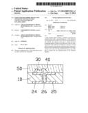
1. A light emitting diode comprising: a substrate consisting two
separated parts with a gap therebetween; a first electrical connecting
portion fixed to one of the two separated parts of the substrate and
adjacent to the gap; a second electrical connecting portion fixed to the
other one of the two separated parts of the substrate and adjacent to the
gap; an LED chip mounted on the substrate and electrically connected to
the first and second electrical connecting portions; and an encapsulation
covering the LED chip and fill in at least a part of the gap to connect
the two separated parts of the substrate together.
2. The light emitting diode of claim 1 wherein the LED chip is electrically connected to the first and second electrical connecting portions by wire bonding of metal wires.
3. The light emitting diode of claim 2, wherein the encapsulation also covers the metal wires.
4. The light emitting diode of claim 1, wherein the encapsulation fills the gap completely.
Description:
CROSS-REFERENCE TO RELATED APPLICATIONS
[0001] This patent application is a divisional application of U.S. patent application Ser. No. 13/332,380, filed on Dec. 21, 2011, entitled "METHOD FOR MANUFACTURING LIGHT EMITTING DIODES INCLUDING FORMING CIRCUIT STRUCTURES WITH A CONNECTING SECTION", assigned to the same assignee, and claiming foreign priority of China patent application No. 201110104678.0 filed on Apr. 26, 2011. The disclosures of the copending U.S. patent application and the China patent application are incorporated herein by reference in their entireties.
BACKGROUND
[0002] 1. Technical Field
[0003] The present disclosure relates to a method for manufacturing semiconductor lighting devices, and particularly, to a method for manufacturing light emitting diodes. The present disclosure also relates to light emitting diodes obtained by the method.
[0004] 2. Description of Related Art
[0005] Light emitting diodes (LEDs) have many beneficial characteristics, including low electrical power consumption, low heat generation, long lifetime, small volume, good impact resistance, fast response and excellent stability.
[0006] In general, the LEDs are formed by dividing an LED wafer. The LED wafer includes a substrate, LED chips arranged on the substrate and an encapsulation covering the LED chips. An upper surface and a bottom surface of the substrate have metal electrodes formed thereon. In manufacture of the LEDs, the metal electrodes have to be etched to insulate from each other. In addition, a plurality of holes are defined in the substrate and filled with electrical conductive materials to electrically connect the metal electrodes on the upper surface and lower surface of the substrate. The process wastes a lot of time and the yielding rate of the LEDs is relatively low.
[0007] What is needed is a method for manufacturing LEDs which can ameliorate the problems of the prior art.
BRIEF DESCRIPTION OF THE DRAWINGS
[0008] Many aspects of the disclosure can be better understood with reference to the following drawings. The components in the drawings are not necessarily drawn to scale, the emphasis instead being placed upon clearly illustrating the principles of the disclosure. Moreover, in the drawings, like reference numerals designate corresponding parts throughout the several views.
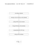
[0009] FIG. 1 is a flow chart of a method for manufacturing LEDs according to an exemplary embodiment of the present disclosure.
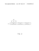
[0010] FIG. 2 is a cross sectional view showing a semi-finished product obtained from a first step and a second step of the method in FIG. 1.
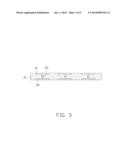
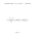
[0011] FIGS. 3-4 are views similar to FIG. 2, showing the semi-finished product obtained after a third step of the method in FIG. 1.
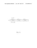
[0012] FIG. 5 is a view similar FIG. 2, showing the semi-finished product obtained after a fourth step of the method in FIG. 1.
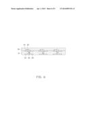
[0013] FIG. 6 is a view similar FIG. 2, showing the semi-finished product obtained after a fifth step of the method in FIG. 1.
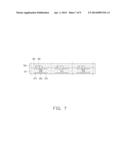
[0014] FIG. 7 is a view similar FIG. 2, showing the semi-finished product obtained after a sixth step of the method in FIG. 1.
[0015] FIG. 8 is a view similar FIG. 2, showing an LED manufactured by the method in FIG. 1.
[0016] FIG. 9 shows a top view of the LED of FIG. 8.
DETAILED DESCRIPTION
[0017] An embodiment of the present disclosure will now be described in detail below, with reference to the accompanying drawings.
[0018] FIG. 1 shows a flow chart of a method for manufacturing an LED according to an exemplary embodiment of the present disclosure. The method for manufacturing the LED includes following steps: providing a substrate; forming a circuit structure on the substrate; cutting the circuit structure; fixing LED chips on the substrate; encapsulating the LED chips; and cutting the substrate. Details are given below.
[0019] Referring to FIG. 2, firstly, the substrate 10 is provided. The substrate 10 can be made of a material selected from a group consisting of sapphire, ZnO, silicate, and ceramic. In this embodiment, the substrate 10 has a plurality of concaves respectively formed in an upper surface and a bottom surface thereof. The concaves are in a uniform interval. A plurality of through holes extends through the substrate 10. Each through hole is aligned with and communicates with one concave in the upper surface (upper concave) and one concave in the bottom surface (bottom concave) of the substrate 10. The through hole and corresponding upper concave and bottom concave cooperatively form a receiving space.
[0020] Then, a plurality of circuit structures 20 are formed on the substrate 10 in a uniform interval. Each of the circuit structure 20 includes a first metal layer 21, a second metal layer 22 and a connecting section 23 interconnecting the first metal layer 21 with the second metal layer 22. The first metal layer 21 and the second metal layer 22 are arranged on the upper surface and the bottom surface of the substrate 10 respectively, and paralleled to and vertically aligned with each other. In this embodiment, each circuit structure 20 is filled on one receiving space, with the first metal layer 21 filled in the upper concave, the second metal layer 22 filled in the bottom concave, and the connecting section 23 filled in the through hole. An upper surface of the first metal layer 21 is coplanar with the upper surface of the substrate 10, and a bottom surface of the second metal layer 22 is coplanar with the bottom surface of the substrate 10. In this embodiment, the circuit structures 20 can be formed by insert molding technology. In an alternative embodiment, the circuit structures 20 can also be formed by sputtering, vacuum evaporating or electroplating. The circuit structure 20 can be made of a material selected from a group consisting of Al (aluminum), Cu (copper), and Ag (sliver).
[0021] Then, referring to FIGS. 3-4, each of the circuit structures 20 is cut through along the connecting section 23, thereto form a first electrical connecting portion 24 and a second electrical connecting portion 25 insulated from each other. In addition the substrate 10 is separated into a plurality of parts. The first electrical connecting portion 24 and the second electrical connecting portion 25 each extend from the upper surface to the bottom surface of the substrate 10, thereto form a surface-mounting structure. A gap 26 is formed between adjacent first electrical connecting portion 24 and second electrical connecting portion 25. In this embodiment, a width of the gap 26 is not less than 0.1 mm. In addition, in forming the circuit structures 20, indentations (not shown) can previously be formed in the positions needed to be cut off. Cross sections of the indentations can be V-shaped, arch-shaped or square-shaped.
[0022] Referring to FIG. 5, a plurality of LED chips 30 is formed on the substrate 10, and particularly on the upper surfaces of the first electrical connecting portions 24. The LED chips 30 can be made of a material selected from a group consisting of GaN, InGaN, AlInGaN, and GaP. Each LED chip 30 is secured to a corresponding first electrical connecting portion 24 by gluing of adhesive, and is electrically connected to the corresponding first electrical connecting portion 24 and second electrical connecting portion 25 by wire bonding of gold wires 40.
[0023] Referring to FIG. 6, then an encapsulation 50 is formed on the substrate 10 and encapsulating all of the LED chips 30 and the gold wires 40. The encapsulation 50 is made of transparent materials such as epoxy resin, polycarbonate (PC) and polymethyl methacrylate (PMMA). The encapsulation 50 is doped with phosphors (not shown), thereto change the color of light emitted by the LED chip 30. The phosphors can be made of garnets, silicates, nitrides or nitrogen oxides. The encapsulation 50 covers the upper surface of the substrate 10, the upper surfaces of the first electrical connecting portions 24 and the upper surfaces of the second electrical connecting portions 25 and fills in the gaps 26, thereto isolate the LED chips 30 from the external environment. The gaps 26 can be fully filled with the encapsulation 50, or be partly filled with the encapsulation 50, whereby the separated parts of the substrate 10 are connected together by the encapsulation 50.
[0024] Finally, referring to FIG. 7, the semi-finished product is severed along paths between the first electrical connecting portion 24 and the second electrical connecting portion 25 of neighboring circuit structures 20 through the substrate 10 and the encapsulation 50 in a direction perpendicular to the substrate 10, thereto form a plurality of individual LEDs as shown in FIGS. 8-9.
[0025] As described above, the method for manufacturing the LEDs includes a step of forming circuit structure 20 on the substrate 10. The circuit structure 20 includes the first metal layer 21 formed on the upper surface of the substrate 10, the second metal surface 22 formed on the bottom surface of the substrate 10 and the connecting section 23 extending through the substrate 10 and connecting the first metal layer 21 with the second metal layer 22. Then the circuit structure 20 is cut through along a middle of the connecting section 23 in a direction particular to the substrate 10, thereto form the first electrical connecting portion 24 and the second electrical connecting portion 25 insulated from each other. A gap 26 is formed between adjacent first electrical connecting portion 24 and second electrical connecting portion 25. LED chips 30 are adhered to the first electrical connecting portions 24, respectively, and electrically connected to the first and second electrical connecting portions 24 by wire bonding. Encapsulation 50 is applied on the upper surface of the substrate 10 to encapsulate the LED chips 30 and fill in the gaps 26 to obtain a semi-finished product. Finally, the semi-finished product is severed along paths between the first electrical connecting portions 24 and the second electrical connecting portions 25 between neighboring circuit structures 20 through the encapsulation 50 and the substrate 10 in a direction particular to the substrate 10 to obtain the LEDs. The method for manufacturing the LEDs described above is simple and easy to operate. Thus, the yielding rate of the LEDs is high.
[0026] While certain embodiments have been described and exemplified above, various other embodiments will be apparent to those skilled in the art from the foregoing disclosure. The disclosure is not limited to the particular embodiments described and exemplified, and the embodiments are capable of considerable variation and modification without departure from the scope and spirit of the appended claims.
User Contributions:
Comment about this patent or add new information about this topic:
Images included with this patent application:
 |  |
 |  |
 |  |
 |  |
 |  |
| New patent applications in this class: | |
| Date | Title |
|---|---|
| 2019-05-16 | Optoelectronic device and the manufacturing method thereof |
| 2019-05-16 | Light emitting element including metal bulk |
| 2019-05-16 | Ultraviolet light emitting diode |
| 2019-05-16 | Light-emitting device |
| 2018-01-25 | Display device and method of manufacturing the same |
| New patent applications from these inventors: | |
| Date | Title |
|---|---|
| 2016-04-28 | Led package with reflecting cup |
| 2014-10-16 | Method for manufacturing light emitting diode packages |
| 2014-07-31 | Light emitting diode package with oxidation-resistant metal coating layer |
| 2014-06-19 | Lead frame and light emitting diode package having the same |
| 2014-04-10 | Led device |
| Top Inventors for class "Active solid-state devices (e.g., transistors, solid-state diodes)" | |
| Rank | Inventor's name |
|---|---|
| 1 | Shunpei Yamazaki |
| 2 | Shunpei Yamazaki |
| 3 | Kangguo Cheng |
| 4 | Huilong Zhu |
| 5 | Chen-Hua Yu |