Patent application title: UNIVERSAL SERIAL BUS SIGNAL TEST DEVICE
Inventors:
Jie Chen (Shenzhen, CN)
Jie Chen (Shenzhen, CN)
Assignees:
HON HAI PRECISION INDUSTRY CO., LTD.
HONG FU JIN PRECISION INDUSTRY (ShenZhen) CO., LTD.
IPC8 Class: AG06F1340FI
USPC Class:
710314
Class name: Bus interface architecture bus bridge common protocol (e.g., pci to pci)
Publication date: 2014-03-27
Patent application number: 20140089554
Abstract:
A universal serial bus (USB) signal test device includes a printed
circuit board. A first connector, a second connector, and a number of USB
hub integrated circuit (ICs) are arranged on the printed circuit board.
The USB hub ICs are connected in series. A USB signal is passed through
the USB hub ICs and an auxiliary test device in that order. The USB
signals are measured with an oscilloscope after being passed through the
USB hub ICs and the auxiliary test device.Claims:
1. A universal serial bus (USB) signal test device, comprising: a printed
circuit board (PCB); a first connector arranged on the PCB and
connectable to a test device to receive USB signals from the test device;
a plurality of USB hub integrated circuits (ICs) connected in series,
wherein each of the USB hub IC comprises a first group of pins and a
second group of pins; the first group of pins of a first one of the
plurality of USB hub ICs is connected to the first connector, the first
group of pins of another USB hub IC is connected to the second group of
pins of an adjacent previous USB hub IC; a second connector connected to
the second group of pins of a last one of the plurality of USB hub ICs to
output the USB signals; a power connector connected to a power pin of
each of the plurality of USB hub ICs; a clock generator connected to a
clock pin of each of the plurality of USB hub ICs.
2. The USB signal test device of claim 1, further comprising a plurality of USB connectors, wherein each of the plurality of USB hub ICs comprises a third group of pins, the third group of pins of each USB hub IC is connected to a corresponding one of the plurality of USB connectors.
3. The USB signal test device of claim 1, wherein the connection of the first and second groups of pins of the plurality of USB hub ICs are through traces on the PCB.
Description:
BACKGROUND
[0001] 1. Technical Field
[0002] The present disclosure relates to a universal serial bus (USB) signal test device.
[0003] 2. Description of Related Art
[0004] In USB signal integrity testing, according to test standards, a test signal should be transmitted six times. Typically, five USB hubs and an auxiliary test device are used to transmit the test signal for six times. However, all devices are manually connected in this testing method, which is inconvenient and easily causes error.
[0005] Therefore, there is room for improvement in the art.
BRIEF DESCRIPTION OF THE DRAWINGS
[0006] Many aspects of the present disclosure can be better understood with reference to the following drawing(s). The components in the drawing(s) are not necessarily drawn to scale, the emphasis instead being placed upon clearly illustrating the principles of the present disclosure. Moreover, in the drawing(s), like reference numerals designate corresponding parts throughout the several views.
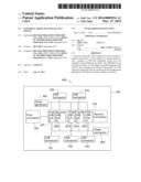
[0007] FIG. 1 is a block diagram of an embodiment of a universal serial bus (USB) signal test device of the present disclosure.
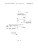
[0008] FIG. 2 is a block diagram of the USB signal test device of FIG. 1 in use.
DETAILED DESCRIPTION
[0009] FIG. 1 shows an embodiment of a universal serial bus (USB) signal test device 600 of the present disclosure.
[0010] The USB signal test device 600 includes a printed circuit board (PCB) 100. A first connector 700, a second connector 706, and first to fifth USB hub integrated circuits (IC) 601-605 are on the PCB 100. The first to fifth USB hub IC 601-605 are connected in series. Each of the first to fifth USB hub IC 601-605 includes three groups of pins used to transmit USB signals. A first group of pins of the first USB hub IC 601 are connected to the first connector 700. A second group of pins of the first USB hub IC 601 are connected to a first group of pins of the second USB hub IC 602. A third group of pins of the first USB hub IC 601 are connected to a USB connector 701. A second group of pins of the second USB hub IC 602 are connected to a first group of pins of the third USB hub IC 603. A third group of pins of the second USB hub IC 602 are connected to a USB connector 702. A second group of pins of the third USB hub IC 603 are connected to a first group of pins of the fourth USB hub IC 604. A third group of pins of the third USB hub IC 603 are connected to a USB connector 703. A second group of pins of the fourth USB hub IC 604 are connected to a first group of pins of the fifth USB hub IC 605. A third group of pins of the fourth USB hub IC 604 are connected to a USB connector 704. A second group of pins of the fifth USB hub IC 605 are connected to the second connector 706. A third group of pins of the fifth USB hub IC 605 are connected to a USB connector 705. Each of the first to fifth USB hub IC 601-605 includes a clock pin connected to a clock generator 801 to ensure the operation sequences of the first to fifth USB hub IC 601-605 are the same. Each of the first to fifth USB hub IC 601-605 includes a power pin connected to a power connector 802 to receive the operation voltage. The above-mentioned connection of the pins of the first to fifth USB hub IC 601-605 are achieved by means of traces on the PCB 100. The USB connectors 701-705, the first connector 700, and the second connector 706 are used to connect peripheral devices. The power connector 802 is used to connect a power supply.
[0011] FIG. 2 is a block diagram of the USB signal test device in use.
[0012] The USB signal test device 600 is connected to a test device 500 through the first connector 700 to receive USB signals from the test device. The USB signal test device 600 is connected to an auxiliary test device 200. The auxiliary test device 200 includes a USB hub and a test connector. The USB hub includes a first USB connector 201 (labeled A in FIG. 2) and a second USB connector 202 (labeled B in FIG. 2). The first USB connector 201 is connected to the second connector 706. The second USB connector 202 is connected to a third USB connector 401 (labeled C in FIG. 2) of a motherboard 400. An oscilloscope 300 is connected to a test terminal of the auxiliary test device 200.
[0013] In the embodiment, the USB signal is passed through the first to fifth USB hub IC 601-605 and the auxiliary test device 200 in that order. The oscilloscope 300 will measure the signal transmitted for six times. In another embodiment, the first USB connector 201 can be connected to the USB connector 702. The oscilloscope 300 measures the signal transmitted for three times.
[0014] While the disclosure has been described by way of example and in terms of preferred embodiment, it is to be understood that the disclosure is not limited thereto. To the contrary, it is intended to cover various modifications and similar arrangements as would be apparent to those skilled in the art. Therefore, the range of the appended claims should be accorded the broadest interpretation so as to encompass all such modifications and similar arrangements.
User Contributions:
Comment about this patent or add new information about this topic:
| People who visited this patent also read: | |
| Patent application number | Title |
|---|---|
| 20140089068 | Videos for In Application Purchases and Rewards for Sharing Same through Social Media and Video Advertising for Reengagement |
| 20140089067 | USER REWARDS FROM ADVERTISERS FOR CONTENT PROVIDED BY USERS OF A SOCIAL NETWORKING SERVICE |
| 20140089066 | METHODS FOR MANAGING REFERRALS AND DEVICES THEREOF |
| 20140089065 | DISK DISPENSING AND RETRIEVAL SYSTEM AND ASSOCIATED METHODS |
| 20140089064 | SYSTEMS AND METHODS FOR TRANSFERRING ELECTRICAL ENERGY BETWEEN VEHICLES |
Images included with this patent application:
 |  |
 |
| Similar patent applications: | |
| Date | Title |
|---|---|
| 2014-05-01 | Power supply circuit for universal serial bus interface |
| 2014-01-02 | Universal serial bus repeater |
| 2014-01-09 | Universal digital block interconnection and channel routing |
| 2014-01-02 | Method for operating a handheld computer by usb input devices |
| 2014-01-09 | Method and apparatus for identifying wireless peripherals and their states at a docking host for wireless docking |
| New patent applications in this class: | |
| Date | Title |
|---|---|
| 2016-12-29 | Multiple transaction data flow control unit for high-speed interconnect |
| 2016-07-07 | System and method for a low emission network |
| 2016-06-02 | Electronic device and electronic device assembly |
| 2016-03-03 | Server comprising a plurality of modules |
| 2016-02-04 | Pci express cluster |
| New patent applications from these inventors: | |
| Date | Title |
|---|---|
| 2022-08-25 | Signal sending method and device, signal receiving method and device, information feedback method and device, communication node, and medium |
| 2022-01-13 | Artificial intelligence-based wakeup word detection method and apparatus, device, and medium |
| 2021-10-21 | Manufacturing method of color film substrate and color film substrate |
| 2017-01-26 | Method and device for compressing local feature descriptor, and storage medium |
| 2016-04-14 | Air deflection system |
| Top Inventors for class "Electrical computers and digital data processing systems: input/output" | |
| Rank | Inventor's name |
|---|---|
| 1 | Daniel F. Casper |
| 2 | John R. Flanagan |
| 3 | Matthew J. Kalos |
| 4 | Mahesh Wagh |
| 5 | David J. Harriman |