Patent application title: ALTERNATING TRAVELING-WAVE MACH-ZEHNDER MODULATOR
Inventors:
Christopher Doerr (Maynard, MA, US)
IPC8 Class: AG02F101FI
USPC Class:
385 3
Class name: Temporal optical modulation within an optical waveguide electro-optic phase modulation type
Publication date: 2013-12-26
Patent application number: 20130343693
Abstract:
Disclosed herein is a traveling-wave Mach-Zehnder modulator and method of
operating same that advantageously exhibits a reduced optical insertion
loss as compared with contemporary Mach-Zehnder structures. Such
advantage comes at the modest expense of increased modulator length and
increased RF loss.Claims:
1. A method of driving a two-arm, traveling-wave Mach-Zehnder modulator
comprising the steps of: applying a drive voltage to the Mach-Zehnder
modulator such that it alternates between one arm and the other arm.
2. A two-arm, traveling-wave Mach-Zehnder modulator comprising: a first optical waveguide associated with the first one of the arms; a second optical waveguide associated with the second one of the arms; a traveling wave electrode that applies a modulated electrical field to a portion of the first optical waveguide; and a second traveling wave electrode that applies modulated electrical field to a portion of the second optical waveguide; wherein said traveling wave electrodes are driven alternately and not simultaneously.
Description:
CROSS REFERENCE TO RELATED APPLICATIONS
[0001] This application claims the benefit of U.S. Provisional Patent Application Ser. No. 61/664,618 filed Jun. 26, 2012 which is incorporated by reference in its entirety as if set forth at length herein.
TECHNICAL FIELD
[0002] This disclosure relates generally to the field of optical communications and in particular to a traveling-wave Mach-Zehnder modulator.
BACKGROUND
[0003] Contemporary optical communications and other systems oftentimes make extensive use of Mach-Zehnder modulators. Given their importance, improved Mach-Zehnder structures would represent a welcome addition to the art.
SUMMARY
[0004] An advance in the art is made according to an aspect of the present disclosure directed to a traveling-wave Mach-Zehnder modulator that advantageously exhibits a reduced optical insertion loss as compared with contemporary Mach-Zehnder structures. Such advantage comes at the modest expense of increased modulator length and increased RF loss.
[0005] Operationally, and according to an aspect of the present disclosure, a full voltage of a differential line is applied across one diode at a time thereby driving the two arms of the Mach-Zehnder modulator alternately--in sharp contrast to the prior art which drives the two arms simultaneously.
[0006] Advantageously, such operation according to the present disclosure reduces the overall optical insertion loss due to the active region(s) b a factor of two in dB. Such advantage comes at modest cost namely, the modulator according to the present disclosure will be approximately twice as long if the same capacitance per unit length is desired, and the total RF loss at the end of a transmission line is higher due to the higher total capacitance.
BRIEF DESCRIPTION OF THE DRAWING
[0007] A more complete understanding of the present disclosure may be realized by reference to the accompanying drawings in which:
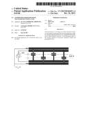
[0008] FIG. 1 shows a schematic of a prior art Mach-Zehnder modulator wherein optical waveguides are represented by dotted lines; and
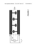
[0009] FIG. 2 shows a schematic of a traveling-wave Mach-Zehnder modulator according to an aspect of the present disclosure wherein optical waveguides are represented by dotted lines.
DETAILED DESCRIPTION
[0010] The following merely illustrates the principles of the disclosure. It will thus be appreciated that those skilled in the art will be able to devise various arrangements which, although not explicitly described or shown herein, embody the principles of the disclosure and are included within its spirit and scope.
[0011] Furthermore, all examples and conditional language recited herein are principally intended expressly to be only for pedagogical purposes to aid the reader in understanding the principles of the disclosure and the concepts contributed by the inventor(s) to furthering the art, and are to be construed as being without limitation to such specifically recited examples and conditions.
[0012] Moreover, all statements herein reciting principles, aspects, and embodiments of the disclosure, as well as specific examples thereof, are intended to encompass both structural and functional equivalents thereof. Additionally, it is intended that such equivalents include both currently-known equivalents as well as equivalents developed in the future, i.e., any elements developed that perform the same function, regardless of structure.
[0013] Thus, for example, it will be appreciated by those skilled in the art that the diagrams herein represent conceptual views of illustrative structures embodying the principles of the invention.
[0014] In addition, it will be appreciated by those skilled in art that any flow charts, flow diagrams, state transition diagrams, pseudocode, and the like represent various processes which may be substantially represented in computer readable medium and so executed by a computer or processor, whether or not such computer or processor is explicitly shown.
[0015] In the claims hereof any element expressed as a means for performing a specified function is intended to encompass any way of performing that function including, for example, a) a combination of circuit elements which performs that function or b) software in any form, including, therefore, firmware, microcode or the like, combined with appropriate circuitry for executing that software to perform the function. The invention as defined by such claims resides in the fact that the functionalities provided by the various recited means are combined and brought together in the manner which the claims call for. Applicant thus regards any means which can provide those functionalities as equivalent as those shown herein. Finally, and unless otherwise explicitly specified herein, the drawings are not drawn to scale.
[0016] Thus, for example, it will be appreciated by those skilled in the art that the diagrams herein represent conceptual views of illustrative structures embodying the principles of the disclosure.
[0017] By way of some additional background, it is noted that differentially driven traveling-wave Mach-Zehnder modulators (MZMs) have proven to be quite useful for creating advanced modulation formats with high fidelity and low driver power. Such modulators have particularly proven their utility in InP photonics, Si photonics and other electro-optic material systems.
[0018] A representative prior-art design of a traveling-wave Mach-Zehnder modulator is shown schematically in FIG. 1 wherein dotted lines represent optical waveguides. As may be observed from that Figure, the prior art modulator comprises a main RF coplanar strip waveguide with capacitive loading. (See., e.g., Y. Cui, "Modeling and Design of GaAs traveling-wave electrooptic modulators based on capacitively loaded coplanar strips" Journal of Lightwave Technology, vol. 24, no. 1, pp. 544-554, 2006) the entire contents of which are hereby incorporated by reference in its entirety. With such structures, two arms of the MZM are differentially driven with structures that connect to a main line. The modulator(s), such as InP or Si modulators, are constructed as diodes. Two diodes associated with the two MZM arms are connected in series. One known advantage of this design is that it is simple and the capacitance is low due--in part--to having the two diodes connected in series. One disadvantage of such an arrangement is that the voltage is reduced by a factor of two across each diode because of the series arrangement. Consequently, an active region of such modulators must be long in order to achieve a desired phase shift. Of further disadvantage, the active region of such modulators typically exhibit a high optical loss.
[0019] According to an aspect of the present disclosure, an advance is made in the art by applying the full voltage of the differential line across one diode at a time--thereby driving the two arms alternately rather than simultaneously as done in the prior art.
[0020] As noted previously, such advance comes at a modest cost namely, a modulator according to the present disclosure will be approximately twice as long if the same capacitance per unit length is desired, and the total RF loss at the end of a transmission line is higher due to the higher total capacitance
[0021] Turning now to FIG. 2, there it shows a traveling-wave Mach-Zehnder modulator in schematic form according to an aspect of the present disclosure. As shown, a coplanar microstrip includes--in addition to two main lines--two auxiliary lines that exhibit a different DC level than the two main lines for biasing the diodes. These extra--auxiliary--lines are connected to the main lines with a high capacitance. As may be appreciated, the auxiliary lines may be placed laterally or vertically relative to the main lines.
[0022] According to an aspect of the present disclosure, because the capacitance in the active regions is effectively doubled, if one needs a same average capacitance per unit length as prior art designs, then loading of the line by the active section must be reduced by a factor of two.
[0023] As may be appreciated if the capacitance per unit length and V.sub.πL of each diode are c0 V.sub.πL, respectively, then the total modulator length for the prior art design required for full binary phase-shift keying (BPSK) is defined by:
L = c 0 V π L c d V pp ; ##EQU00001##
where cd is the desired capacitance per unit length, and VPP is the differential peak-to-peak drive voltage. For designs according to the present disclosure:
L = 2 c 0 V π L c d V pp ; ##EQU00002##
Thus, designs according the present disclosure will be twice as long as prior art designs.
[0024] Furthermore, if the optical loss in dB per unit length of the active regions is a then the total loss of prior art designs may be represented by:
loss = 2 V π L V pp α ; ##EQU00003##
whereas for alternating designs according to the present disclosure it is represented by:
loss = V π L V pp α ##EQU00004##
[0025] As may be observed by these relationships, the loss is reduced b a factor of two in designs according to the present disclosure.
[0026] If however, the RF loss is dominated by series resistance in the connections to the diodes, then designs according to the present disclosure will exhibit twice the RF loss at the end of a modulator because the total capacitance is twice as large.
[0027] Accordingly, alternating designs according to the present disclosure decrease the optical loss significantly however increase the total capacitance. This increased capacitance results in a longer modulator and increased RF loss. Consequently, alternating designs according to the present disclosure may be particularly well suited for lower speed operation, where such issues present less concern. Additionally, such designs may be particularly useful in a resonant modulator, in which a low optical loss is important.
[0028] Those skilled in the art will readily appreciate that while the methods, techniques and structures according to the present disclosure have been described with respect to particular implementations and/or embodiments, those skilled in the art will recognize that the disclosure is not so limited. Accordingly, the scope of the disclosure should only be limited by the claims appended hereto.
User Contributions:
Comment about this patent or add new information about this topic:
Images included with this patent application:
 |  |
| Similar patent applications: | |
| Date | Title |
|---|---|
| 2011-08-11 | Mach-zehnder modulator |
| 2012-02-02 | Mach-zehnder modulator |
| 2011-01-13 | Mach zehnder modulator |
| 2010-10-21 | Planar lightwave apparatus |
| 2011-11-03 | Multi-configurable splice holder |
| New patent applications in this class: | |
| Date | Title |
|---|---|
| 2022-05-05 | Optical modulator |
| 2019-05-16 | Calibration for an optical device |
| 2018-01-25 | Fpc-attached optical modulator and optical transmission device using the same |
| 2018-01-25 | Optical modulator and method of manufacturing same |
| 2017-08-17 | Photonic transmitter |
| New patent applications from these inventors: | |
| Date | Title |
|---|---|
| 2022-01-13 | Optical waveguide passivation for moisture protection |
| 2015-12-10 | Monolithic silicon coherent transceiver with integrated laser and gain elements |
| 2015-10-22 | Integrated polarization filter and tap coupler |
| 2015-07-30 | Wafer-scale testing of photonic integrated circuits using horizontal spot-size converters |
| 2015-07-30 | Silicon depletion modulators with enhanced slab doping |
| Top Inventors for class "Optical waveguides" | |
| Rank | Inventor's name |
|---|---|
| 1 | James Phillip Luther |
| 2 | Trevor D. Smith |
| 3 | Ming-Jun Li |
| 4 | Micah Colen Isenhour |
| 5 | Dennis Michael Knecht |