Patent application title: METHOD OF SUPPRESSING ELECTROMAGNETIC INTERFERENCE EMISSION
Inventors:
Mark Telefus (Orinda, CA, US)
IPC8 Class: AH02M112FI
USPC Class:
363 2112
Class name: Single-ended, separately-driven type with automatic control of the magnitude of output voltage or current for flyback-type converter
Publication date: 2013-12-12
Patent application number: 20130329467
Abstract:
An EMI emission suppressing system, apparatus and method that enables the
EMI produced by high frequency switching of a switching circuit to be
suppressed via the transfer of the higher order harmonic emissions to a
frequency range below the standard EMI bandwidth of less than 150 KHz by
applying low frequency modulation or jitter into the feedback of a
switching signal of the switching circuit. The EMI suppression is
achieved with minimal added ripple on the output signal of the switching
circuit by using discontinuous modulations in the form of only applying
the low frequency modulation when the switch or higher order harmonic
producing element of the switching circuit is accessing, or drawing power
from, the main power supply.Claims:
1. A method of regulating a power converter having a switching circuit,
the method comprising: a. selectively drawing power from a power supply
according to a control signal used to drive the switching circuit; b.
generating a low frequency modulation signal when the switching circuit
draws power from the power supply; and c. applying the low frequency
modulation signal so as to generate a modulated control signal that is
modulated according to the low frequency modulation signal.
2. The method of claim 1 wherein the modulated control signal substantially reduces higher order harmonic emissions corresponding to switching of the switching element.
3. The method of claim 1 wherein the low frequency modulation signal is generated at a predetermined frequency.
4. The method of claim 3 wherein the predetermined frequency comprises a frequency in the range of 2 to 9 Khz.
5. The method of claim 1 applying the low frequency modulation signal comprises: a. generating a modulated error signal that is modulated according to the low frequency modulation signal; and b. supplying the modulated error signal to a controller circuit of the switching circuit, wherein the controller circuit generates the modulated control signal.
6. The method of claim 1 wherein the control signal comprises a pulse width modulated signal for controlling a duty cycle of the switching circuit.
7. The method of claim 1 further comprising regulating an output voltage of the power converter.
8. The method of claim 7 further comprising supplying a feedback signal to the switching circuit, wherein the feedback signal is representative of the output voltage.
9. The method of claim 1 further comprising discontinuing generation of the low frequency modulation signal when the switching circuit is not drawing power from the power supply.
10. The method of claim 1 wherein driving the switching circuit with the modulated control signal substantially reduces harmonic distribution in a switching frequency of the switching circuit.
11. A method of regulating a power converter having a switching circuit, the method comprising: a. selectively drawing power from a power supply according to a control signal used to drive the switching circuit; b. generating a low frequency modulation signal; and c. applying the low frequency modulation signal when the switching circuit draws power from the power supply so as to generate a modulated control signal that is modulated according to the low frequency modulation signal.
12. The method of claim 11 wherein the modulated control signal substantially reduces higher order harmonic emissions corresponding to switching of the switching element.
13. The method of claim 11 wherein the low frequency modulation signal is generated at a predetermined frequency.
14. The method of claim 13 wherein the predetermined frequency comprises a frequency in the range of 2 to 9 Khz.
15. The method of claim 11 applying the low frequency modulation signal comprises: a. generating a modulated error signal that is modulated according to the low frequency modulation signal; and b. supplying the modulated error signal to a controller circuit of the switching circuit, wherein the controller circuit generates the modulated control signal.
16. The method of claim 11 wherein the control signal comprises a pulse width modulated signal for controlling a duty cycle of the switching circuit.
17. The method of claim 11 further comprising regulating an output voltage of the power converter.
18. The method of claim 17 further comprising supplying a feedback signal to the switching circuit, wherein the feedback signal is representative of the output voltage.
19. The method of claim 11 further comprising discontinuing application of the low frequency modulation signal when the switching circuit is not drawing power from the power supply.
20. The method of claim 11 wherein driving the switching circuit with the modulated control signal substantially reduces harmonic distribution in a switching frequency of the switching circuit.
21. A method of regulating a power converter having a switching circuit, the method comprising: a. injecting a low frequency modulation signal into a summation circuit configured to output an error signal; b. modulating the error signal of the summation circuit using the low frequency modulation signal when the switching circuit is drawing power from a power supply; and c. using the modulated error signal to substantially reduce harmonic distribution in a switching frequency of the switching circuit.
22. The method of claim 21 further comprising generating the low frequency modulation signal at a predetermined frequency using a signal generator.
23. The method of claim 22 wherein the predetermined frequency comprises a frequency in the range of 2 to 9 Khz.
24. The method of claim 21, further comprising: a. applying the modulated error signal to a controller circuit for the switching circuit; and b. generating a pulse width modulated signal for controlling a duty cycle of the switching circuit.
25. The method of claim 21 further comprising regulating an output voltage of the power converter.
26. The method of claim 25 further comprising supplying a feedback signal to the summation circuit, wherein the feedback signal is representative of the output voltage.
27. The method of claim 21 further comprising discontinuing modulation of the error signal using the low frequency modulation signal when the switching circuit is not drawing power from the power supply.
Description:
RELATED APPLICATIONS
[0001] This Patent Application claims priority under 35 U.S.C. 119 (e) of the co-pending U.S. provisional application, Ser. No. 61/658,245, filed, Jun. 11, 2012, and entitled "Electromagnetic Interference Emission Suppressor". This application incorporates U.S. provisional application, serial number in its entirety by reference.
FIELD OF THE INVENTION
[0002] The present invention relates to the field of power supplies. More particularly, the present invention relates to a power converter system with modulated control.
BACKGROUND
[0003] Every electrical device that connects with a power supply main is required not to pollute or transmit high frequency noise onto the main. The amount of electrical emission allowed by electrical devices is heavily regulated by the Federal Communications Commission (FCC). Conventional power supply designs have migrated to using higher operating frequencies since the higher operating frequencies allow a reduction in size of power supply components and allow a reduction in cost. The disadvantage of operating at higher frequencies is the increased production of higher order harmonics or electromagnetic interference (EMI).
[0004] Conventional methods of reducing EMI have been aimed at reducing a switching frequency of a switching circuit below standard EMI bandwidth limits of 150 KHz as set by the FCC. This approach has the disadvantage of increasing the size of magnetic components in a power supply. Other methods of reducing EMI have simply been to add additional filter components to reduce unwanted frequency harmonics. This second approach has the disadvantage of adding to the weight, size and cost of power supplies. Another approach to reducing large spikes of harmonics or EMI is the use of a snubber circuit. The snubber circuit although effective in reducing EMI, compromises efficiency of a power converter. In yet another approach, EMI is reduced by using jitter that takes a discrete harmonic spectrum and spreads the EMI over a continuous frequency range. Conventional systems use jitter by injecting noise into a gate drive or controller of the converter. Injecting noise into the gate drive of the converter has the disadvantage of distorting the output voltage signal. Further, injecting noise directly into a gate drive only applies jitter to the rising and falling edges of the converter switching signal. Moreover, because the jitter is continuous throughout the cycles of the switching signal, is outside the bandwidth of the amplifier and is injected outside the regulation loop of the switching circuit, it causes unwanted high ripple on the output of the switching circuit. Accordingly, by continuously injecting jitter directly into the gate drive circuit, conventional power converters inhibit the efficiency of feedback loop and other features including zero voltage switching and sampling of the switching signal.
SUMMARY OF THE INVENTION
[0005] An EMI emission suppressing system, apparatus and method includes a frequency modulation element that modulates the frequency of a switching element when the switching element is drawing power from the main power supply in order to reduce EMI emissions on the main power supply. The frequency modulation element discontinues modulation when the switching element is not drawing power from the main power supply in order to reduce ripple on the load. As a result, the EMI emission suppressing system is able to minimize EMI emissions on the main power supply while not outputting excess ripple on the load.
BRIEF DESCRIPTION OF THE DRAWINGS
[0006] Several example embodiments are described with reference to the drawings, wherein like components are provided with like reference numerals. The example embodiments are intended to illustrate, but not to limit, the invention. The drawings include the following figures:
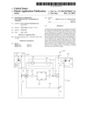
[0007] FIG. 1 illustrates a functional block diagram of an EMI suppression system according to some embodiments.
[0008] FIG. 2 illustrates a circuit diagram of an EMI suppression system according to some embodiments.
[0009] FIG. 3 illustrates a flowchart of a method of suppressing EMI emission according to some embodiments.
[0010] FIG. 4 illustrates a flow chart of a method of suppressing EMI emission according to an alternative embodiment.
DETAILED DESCRIPTION
[0011] Embodiments of the present application are directed to an EMI emission suppressing system, device and method. Those of ordinary skill in the art will realize that the following detailed description of the EMI emission suppressing system, device and method is illustrative only and is not intended to be in any way limiting. Other embodiments of the EMI emission suppressing system, device and method will readily suggest themselves to such skilled persons having the benefit of this disclosure.
[0012] Reference will now be made in detail to implementations of the EMI emission suppressing system, device and method as illustrated in the accompanying drawings. The same reference indicators will be used throughout the drawings and the following detailed description to refer to the same or like parts. In the interest of clarity, not all of the routine features of the implementations described herein are shown and described. It will, of course, be appreciated that in the development of any such actual implementation, numerous implementation-specific decisions must be made in order to achieve the developer's specific goals, such as compliance with application and business related constraints, and that these specific goals will vary from one implementation to another and from one developer to another. Moreover, it will be appreciated that such a development effort might be complex and time-consuming, but would nevertheless be a routine undertaking of engineering for those of ordinary skill in the art having the benefit of this disclosure.
[0013] Embodiments of an EMI emission suppressing system, device and method are described herein. The EMI suppressing system, device and method enables the EMI produced by high frequency switching of a switching circuit to be suppressed via the transfer of the higher order harmonic emissions to a frequency range below the standard EMI bandwidth of less than 150 KHz. The transfer of the higher order harmonic emissions is accomplished by applying low frequency modulation or jitter into the feedback of a switching signal of the switching circuit. Further, this EMI suppression is able to be achieved with minimal added ripple on the output signal by using discontinuous modulations in the form of only applying the low frequency modulation when the switch or higher order harmonic producing element of the switching circuit is accessing or drawing power from the main power supply. As a result, when coupled with the main power supply the low frequency modulation is applied in order to affect the rising and falling edges of switching pulses of the switching circuit thereby substantially reducing EMI noise on the main power supply from the switching circuit. Conversely, when not accessing or drawing power from the main power supply the low frequency modulation is suspended in order to substantially reduce ripple on the output of the switching circuit.
[0014] FIG. 1 illustrates a functional block diagram of an EMI suppressing system 100 according to some embodiments. As shown in FIG. 1, the system 100 includes a power supply 102, a switching element 104, a output circuit 106, a feedback element 108 and a frequency modulation element 110. The power supply 102 is coupled with the switching element 104 which is electrically coupled with the output circuit 106. The feedback element 108 is electrically coupled between the load 106 and frequency modulation element 110 which is electrically coupled with the switching element 104. Alternatively, the feedback element 108 is able to be directly coupled between the output circuit 106 and the switching element 104 and/or the frequency modulation element 110 is able to be electrically coupled with the switching element 104, the feedback element 108 or both.
[0015] The power supply 102 is able to include an AC power supply such as a main line or plug outlet. Alternatively, the power supply 102 is able to include a DC power supply. The switching element 104 is able to include a power converter circuit, such as a flyback converter. Alternatively, the switching element 104 is able to include other types of circuits that include switching elements or otherwise produce EMI emissions. For example, the switching element 104 is able to include a forward converter, a push-pull converter, a half-bridge converter, a full-bridge converter and/or other configurations of switch mode power supplies as are well known in the art. The frequency modulation element 110 is able to include a signal or clock generator. Alternatively, the frequency modulation element 110 is able to include other signal generation or modulation elements that are able to induce low frequency jitter on a signal as are well known in the art. In some embodiments, the frequency modulation element 110 is able to be integrated with the switching element 104, the output circuit 106 and/or the feedback element 108 to form a single integrated circuit. Alternatively, the frequency modulation element 110 is able to include an individual integrated circuit that is able to be coupled to one or more separate circuits such as switching element, output circuit and/or feedback circuits. As a result, the frequency modulation element 110 is able to provide the advantage of being coupled to existing integrated circuits in order to improve their EMI suppression characteristics.
[0016] In operation, the switching element 104 periodically couples to or pulls power from the power supply 102 and supplies a desired output voltage/signal to a load coupled to the output circuit 106. The feedback element 108 detects the output voltage Vout, or a representative value of the output voltage Vout, and adjusts the output of the switching element 104 in order to keep the output voltage Vout within a desired range, thereby regulating the output voltage Vout. In some embodiments, the feedback element 108 adjusts the duty cycle of the switching element 104 in order to control the output voltage Vout. The frequency modulation element 110 detects when the switching element 104 is pulling power from or coupled to the power supply 102 and applies low frequency modulation or jitter to the signal received from the feedback element 108 signal such that EMI caused by the switching element 104 and exposed to the power supply 102 is minimized. The frequency modulation element 110 also detects when the switching element 104 is not pulling power from or is not directly coupled to the power supply 102 and ceases or discontinues to apply low frequency modulation or jitter on the switching element signal in order to minimize ripple on the output voltage/signal applied to the load. In some embodiments, the frequency modulation element 110 performs the detection and modulation within the feedback loop of the switching element 104. As a result, the jitter is only applied when the switching element 104 is coupled to the power supply 102 and the system 100 is able to minimize the amount of EMI transmitted on the power supply 102 from the switching element 104 while also minimizing the amount of ripple induced on the output voltage/signal from the jitter of the frequency modulation element 110.
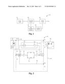
[0017] FIG. 2 illustrates a schematic diagram of an EMI suppression system 200 according to some embodiments. The schematic diagram is substantially similar to the functional block diagram shown in FIG. 1 except the additional details described herein. However, it is understood that alternative schematics are able to be used to implement the functional blocks of FIG. 1. As shown in FIG. 2, the EMI suppression system 200 includes a power supply 202, a switching element 204, an output circuit 206, a feedback element 208 and a frequency modulation element 210. The system 200 is configured to receive an AC voltage signal and to provide a regulated DC output voltage Vout that is suitable for many low voltage appliances such as computer laptops, cell phones and other devices. In some embodiments, the output voltage Vout is able to be within the range 5-40V. Alternatively, the output voltage Vout is able to be less than 5V or more than 40V. In some embodiments, the system 200 is contained on a single integrated circuit. Alternatively, one or more of the components of the suppression system 200 are able to be separate integrated circuits such that the system 200 is formed by multiple integrated circuits electrically coupled together.
[0018] The power supply 202 includes an AC mains power signal that is electrically coupled with a rectifier 212 in order to produce an unregulated DC input voltage Vin that is electrically coupled to both the switching element 204 and the feedback element 208. The output circuit 206 includes a diode D1 and capacitor C1. Alternatively, the output circuit 206 is able to include an output rectifier circuit comprising a half or full-wave rectifier. The feedback element 208 provides a feedback voltage Vfb, which is representative of the output voltage Vout. The frequency modulation element 210 includes the signal generator or clock generator 222 and one or more buffers 216. The switching element 204 includes a transformer T1, a transistor 218, one or more resistors R1, R2, R3, a controller device 214, a summation device 220 and one or more buffers 216. Alternatively, one or more of the summation device 220, the controller device 214 and/or the buffers 216 of the switching element 204 are able to be a part of the frequency modulation element 210 instead of the switching element 204. Indeed, it is understood that one or more of the components of the power supply 202, the switching element 204, the output circuit 206, the feedback element 208 and/or the frequency modulation element 210 are able to be positioned or duplicated on one or more of the other elements 202-210.
[0019] A first end of the transformer T1 is electrically coupled between the input voltage Vin received from the power supply 202 and the drain terminal of the transistor 218. The second end of the transformer T1 is electrically coupled across the diode D1 and capacitor C1 of the output circuit 206. The source terminal of the transistor 218 is electrically coupled with the feedback element 208 and the resistor R3 which is electrically coupled to ground. The Q output line of the controller device 214 is electrically coupled with the gate terminal of the transistor 218 and the input of the signal generator 222 of the frequency modulation element 210 via one or more buffers 216. The S input line of the controller device 214 is electrically coupled with the output of the summation device 220 via another buffer 216. The inputs of the summation device 220 are electrically coupled with the feedback element 208, the output of the signal generator 222, and a reference voltage node Vref that is located between resistors R1 and R2 which are electrically coupled in series between the input voltage Vin and ground. The summation device 220 can be a comparator, an error amplifier or other device that modulates a difference, or error, between the reference voltage Vref and the feedback voltage Vfb, thereby outputting a modulated error signal. In some embodiments, the transformer T1 is a flyback transformer.
[0020] Alternatively, the transformer T1 is able to be other types of transformers or load isolating circuitry as are well known in the art. In some embodiments, the signal generator 222 generates a clock signal at a predetermined frequency, such as in the range of 2.0 to 9.0 KHz. Alternatively, the predetermined frequency is able to be less than 2.0 KHz, greater than 9.0 KHz, or other predetermined frequencies as are well known in the art. In some embodiments, the transistor 218 is a field effect transistor such as a n-type metal-oxide-semiconductor field-effect transistor (MOSFET). Alternatively, the transistor 218 is able to be other types of transistors or switching circuitry as are well known in the art. For example, the switching element 204 is able to include a variable frequency converter, such that an operating bandwidth of the switching element 204 is able to be adjusted depending on output power requirements of the system 200. In some embodiments, the controller device 214 is a SR-NOR latch flipflop. Alternatively, the controller device 214 is able to be other types of flipflops, pulse width modulation circuits or signal logic circuitry able to regulate the duty cycle of the operation of the transistor 218 as are well known in the art.
[0021] In operation, the Q output of the controller device 214 of the switching element 204 outputs a switch control signal, or driving signal, to the gate terminal of the transistor 218 that causes the transistor 218 to repeatedly turn on and off. When the switch control signal is high, it activates the channel of the transistor 218 causing current from the power supply 202 to be drawn through the primary winding of the transformer T and the transistor 2181, through the feedback loop 208 and to ground through resistor R3. When the switch control signal is low, the channel of the transistor 218 is deactivated preventing current flow through the transistor 218 and therefore the primary winding P1, and the voltage across the primary winding P1 goes high and power is transferred to the output circuit 206. The summation device 220 receives a feedback signal from the feedback element 208 and compares the feedback voltage Vfb of the feedback signal to a reference voltage Vref in order to generate an error signal that is input to the S input of the controller device 214 and adjusts the duty cycle of the switch control signal such that a desired output voltage Vout is maintained. As a result, the switching element 204 regulates the output voltage Vout.
[0022] When the switch control signal is high such that the switching element 204 is accessing the power supply 202, the signal generator 222 outputs a low frequency modulation or jitter signal to the summation device 220 such that the error signal is modulated and the modulated error signal is input to the controller device 214 such that the corresponding switch control signal is modulated according to the low frequency modulation/jitter signal. As a result, the EMI caused by the switching element 204 on the power supply 202 is substantially reduced because the modulation of the switch control signal essentially takes the EMI spikes in the switching frequency and reduces and spreads out the EMI spikes over the frequency spectrum. When the switch control signal is low such that the switching element 204 is no longer accessing the power supply and power stored in the transformer T1 is transferred to the output circuit 206, the error signal is no longer modulated with the low frequency modulation signal. In some embodiments, the signal generator 222 only generates the low frequency modulation signal when the switching element 204 is accessing the power supply 202. In other embodiments, the signal generator 222 continuously generates the low frequency modulation signal, but the low frequency modulation signal is only used by the summation device 220 to modulate the error signal when the switching element 204 is accessing the power supply 202. As a result of selectively modulating the error signal and therefore selectively modulating the switching control signal, the ripple on the load caused by the modulated switching control signal is also minimized. Accordingly, the EMI emission suppression system 200 provides the advantage of maintaining maximum reduction of EMI polluted onto the power supply 202 while also minimizing ripple on the output circuit 206.
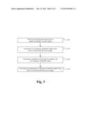
[0023] FIG. 3 illustrates a flow chart of a method of suppressing EMI emission according to some embodiments. The method steps are described in relation to the system elements of FIG. 2. It is understood that the method of suppressing EMI emission can be enabled using alternative system element and configurations. At the step 302, a switching element 204 selectively accesses, or draws power from, a power supply 202 according to a control signal. In some embodiments, accessing the power supply 202 includes drawing current from the power supply 202. For example, accessing the power supply includes activating a transistor 218 which is electrically coupled with the power supply 202, thereby drawing current through the primary winding P1 and the transistor 218. In some embodiments, the control signal for activating the transistor 218 is a pulse width modulated signal output by a controller device 214. In some embodiments, the control signal is adjusted by an error signal generated by a summation device 220 which compares a reference voltage Vref with a feedback signal Vfb. At the step 304, a frequency modulation element 210 generates a low frequency modulation signal, or jitter, when the switching element 204 is accessing the power supply 202. In some embodiments, the low frequency modulation signal is generated at a predetermined frequency in the range of 2.0 to 9.0 KHz. Alternatively, the predetermined frequency is able to be less than 2.0 KHz, greater than 9.0 KHz, or other predetermined frequencies as are well known in the art. At the step 306, a modulated control signal of the switching element 204 is generated according to the low frequency modulation signal. The switching element 204 selectively accesses the power supply 202 according to the modulated control signal thereby minimizing the amount of EMI of the switching element 204 output on the power supply 202. At the step 308, the frequency modulation element 210 discontinues generating the low frequency modulation signal when the switching element 204 is not accessing the power supply 202 so that the control signal is not modulated according to the low frequency modulation signal, thereby minimizing the amount of ripple output on the output circuit 206, where ripple is caused by the modulation or jitter of the modulated control signal. As a result, the method provides the advantage of enabling EMI emission on the power supply to be minimized while also minimizing the amount of ripple on the load.
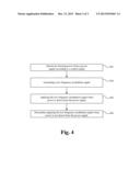
[0024] In an alternative embodiment, the frequency modulation element 210 continuously generates the low frequency modulation signal, but the control signal is only modulated according to the low frequency modulation signal when the switching element 204 is accessing the power supply 202. FIG. 4 illustrates a flow chart of a method of suppressing EMI emission according to this alternative embodiment. At the step 402, the switching element 204 selectively accesses, or draws power from, the power supply 202 according to a control signal. At the step 404, the frequency modulation element 210 generates a low frequency modulation signal, or jitter. At the step 406, the low frequency modulation signal is applied when the switching element accesses the power supply 202, thereby generating a modulated control signal according to the low frequency modulation signal. At the step 408, application of the low frequency modulation signal is discontinued when the switching element 204 is not accessing the power supply 202 so that the control signal is not modulated according to the low frequency modulation signal.
[0025] The method, apparatus and system of EMI emission suppression described herein has many advantages. Specifically, the system minimizes the EMI emission output on a power supply by a switching element by modulating the frequency of the switching element using low frequency modulation in a feedback loop. Further, the system minimizes the ripple output on the load resulting from the low frequency modulation by using discontinuous modulation where the control signal is only modulated when the switching element is accessing the power supply. Thus, the EMI emission suppressor described herein has numerous advantages.
[0026] The EMI emission suppressing system, device and method is described above in terms of modulating a control signal used to regulate an output voltage. It is understood that the EMI emission suppressing system, device and method can alternatively be applied to non-regulating applications. Such alternative applications may or may not include a feedback element. The modulating signal may be applied to a reference or other signal used by the switching element to generate the modulated control signal.
[0027] The present application has been described in terms of specific embodiments incorporating details to facilitate the understanding of the principles of construction and operation of the EMI emission suppressing system, device and method. Many of the components shown and described in the various figures can be interchanged to achieve the results necessary, and this description should be read to encompass such interchange as well. As such, references herein to specific embodiments and details thereof are not intended to limit the scope of the claims appended hereto. It will be apparent to those skilled in the art that modifications can be made to the embodiments chosen for illustration without departing from the spirit and scope of the application.
User Contributions:
Comment about this patent or add new information about this topic:
Images included with this patent application:
 |  |
 |  |
| Similar patent applications: | |
| Date | Title |
|---|---|
| 2013-04-04 | On time sampling prevention |
| 2014-07-03 | Apparatus and method for avoiding transformer saturation |
| 2012-08-09 | Measurement transducer |
| 2013-05-02 | Photovoltaic array emulators |
| 2009-11-05 | System and method for providing adaptive dead times |
| New patent applications in this class: | |
| Date | Title |
|---|---|
| 2022-05-05 | Multi-mode control method for active clamp flyback converter |
| 2017-08-17 | Phase-cut pre-regulator and power supply comprising the same |
| 2016-12-29 | Power conversion device |
| 2016-12-29 | Switching power converter with adaptive power factor correction |
| 2016-12-29 | Integrated circuit and switching power-supply device |
| New patent applications from these inventors: | |
| Date | Title |
|---|---|
| 2022-08-11 | Solid-state circuit interrupters |
| 2021-10-28 | Ac to dc converters |
| 2019-09-12 | Multifunctional system integrator |
| 2014-09-18 | No load detection |
| 2014-09-18 | No load detection and slew rate compensation |
| Top Inventors for class "Electric power conversion systems" | |
| Rank | Inventor's name |
|---|---|
| 1 | Ta-Yung Yang |
| 2 | Lieyi Fang |
| 3 | Alex B. Djenguerian |
| 4 | Martin Fornage |
| 5 | Balu Balakrishnan |