Patent application title: Enhanced Hydrogen Barrier Encapsulation Method for the Control of Hydrogen Induced Degradation of Ferroelectric Capacitors in an F-RAM Process
Inventors:
Shan Sun (Colorado Springs, CO, US)
Thomas E. Davenport (Denver, CO, US)
Assignees:
Ramtron International Corporation
IPC8 Class: AH01L2328FI
USPC Class:
257788
Class name: Active solid-state devices (e.g., transistors, solid-state diodes) encapsulated with specified encapsulant
Publication date: 2013-11-14
Patent application number: 20130300003
Abstract:
A method of encapsulating a ferroelectric capacitor or ferroelectric
memory cell includes forming encapsulation materials adjacent to a
ferroelectric capacitor. forming a ferroelectric oxide (FEO) layer over
the encapsulated ferroelectric capacitor, and forming an FEO
encapsulation layer over the ferroelectric oxide to provide additional
protection from hydrogen induced degradation.Claims:
1. A method of encapsulating a ferroelectric capacitor, comprising:
forming encapsulation materials adjacent to a ferroelectric capacitor;
forming a ferroelectric oxide (FEO) layer over the encapsulated
ferroelectric capacitor; planarizing and polishing the ferroelectric
oxide to a desired thickness by chemical mechanical polishing; and
forming FEO encapsulation materials over the ferroelectric oxide to
provide additional protection from hydrogen induced degradation.
2. The method of claim 1 wherein the FEO encapsulation materials comprise a single material layer.
3. The method of claim 1 wherein the FEO encapsulation materials comprise multiple material layers.
4. The method of claim 1 further comprising performing a recovery anneal.
5. The method of claim 4 further comprising performing the recovery anneal after forming a top electrode contact of the ferroelectric capacitor.
6. (canceled)
7. The method of claim 1 wherein the FEO encapsulation materials are formed by chemical vapor deposition (CVD), atomic layer deposition (ALD), or physical vapor deposition (PVD).
8. The method of claim 1 wherein the FEO encapsulation materials comprise an encapsulation layer and a barrier layer.
9. The method of claim 8 wherein the encapsulation layer comprises CVD AIOx, ALD AIOx, PVD AIOx, CVD SiNx, PVD SiNx, or DVD SiONx.
10. The method of claim 8 wherein the barrier layer comprises CVD AIOx, ALD AIOx, PVD AIOx, CVD SiNx, PVD SiNx, CVD SiONx, PZT, and FEO.
11. The method of claim 8 wherein the encapsulation layer is between 50 and 1000 Angstroms thick.
12. The method of claim 8 wherein the barrier layer is between 50 and 1000 Angstroms thick.
13. The method of claim 1 wherein the ferroelectric oxide comprises TEOS.
14. The method of claim 1 wherein the ferroelectric oxide is between 5000 and 120,000 Angstroms thick.
15. An encapsulated ferroelectric capacitor structure comprising: a ferroelectric capacitor encapsulated with adjacent encapsulation materials; a ferroelectric oxide formed over the encapsulated ferroelectric capacitor; and FEO encapsulation materials formed over the ferroelectric oxide to provide additional protection from hydrogen induced degradation.
16. The encapsulated ferroelectric capacitor structure of claim 15 wherein the FEO encapsulation materials comprise a single material layer.
17. The encapsulated ferroelectric capacitor structure of claim 15 wherein the FEO encapsulation materials comprise multiple material layers.
18. The encapsulated ferroelectric capacitor structure of claim 15 wherein the FEO encapsulation materials comprise an encapsulation layer and a barrier layer.
19. The encapsulated ferroelectric capacitor structure of claim 18 wherein the FEO encapsulation layer comprises CVD AIOx, ALD AIOx, PVD AIOx, CVD SiNx, PVD SiNx, or DVD SiONx.
20. The encapsulated ferroelectric capacitor structure of claim 18 wherein the barrier layer comprises CVD AIOx, ALD AIOx, PVD AIOx, PVD SiNx, CVD SiONx, PZT, and FEO.
21. A method of encapsulating a ferroelectric capacitor, comprising: forming encapsulation materials adjacent to a ferroelectric capacitor; forming a ferroelectric oxide (FEO) over the encapsulated ferroelectric capacitor; planarizing the FEO by chemical mechanical polishing to form a planarized FEO; and forming FEO encapsulation materials over the planarized FEO to provide additional protection from hydrogen induced degradation, wherein the FEO encapsulation materials comprise an encapsulation layer and a barrier layer overlying the encapsulation layer.
Description:
FIELD OF THE INVENTION
[0001] The present invention relates to ferroelectric capacitors and ferroelectric memory cells, and more particularly, to a method of further protecting these capacitors and memory cells from degradation during fabrication.
BACKGROUND OF THE INVENTION
[0002] The conventional hydrogen barrier encapsulation is to deposit encapsulation materials adjacent to ferroelectric capacitors. Such an encapsulation is shown in U.S. Pat. No. 6,249,014. The encapsulation materials can be formed of a single, dual, or partial layers, or combinations thereof. While these known encapsulation techniques can prevent degradation during the manufacturing process, some degradation still occurs. What is desired is a further barrier encapsulation method such that the ferroelectric capacitor or memory cell can be further protected and manufacturing yields can be improved.
SUMMARY OF THE INVENTION
[0003] In the present invention, an additional layer of encapsulation is deposited above the ferroelectric oxide (FEO) to provide additional protection from hydrogen induced degradations. This additional protection is essential to enhance F-RAM yield and reliabilities such as endurance and data retention.
[0004] According to the present invention, a method of encapsulating a ferroelectric capacitor includes forming encapsulation materials adjacent to a ferroelectric capacitor, forming a ferroelectric oxide (FEO) over the encapsulated ferroelectric capacitor, and forming additional encapsulation materials over the ferroelectric oxide to provide additional protection from hydrogen induced degradation. The additional encapsulation is referred to as FEO encapsulation. The FEO encapsulation materials can comprise a single material layer, or multiple material layers. The encapsulation method can include performing a recovery anneal, particularly after forming a top electrode contact of the ferroelectric capacitor. The ferroelectric oxide is polished to a desired thickness by chemical mechanical polishing. The FEO encapsulation materials are formed by chemical vapor deposition (CVD), atomic layer deposition (ALD), or physical vapor deposition (PVD). The FEO encapsulation materials comprise an encapsulation layer and a barrier layer. The encapsulation layer can comprise CVD AlOx, ALD AlOx, PVD AIOx, CVD SiNx, PVD SiNx, or DVD SiONx. The barrier layer can comprise CVD AlOx, ALD AlOx, PVD AlOx, CVD SiNx, PVD SiNx, CVD SiONx, PZT, and FEO. The encapsulation layer is between 50 and 1000 Angstroms thick, and the barrier layer is between 50 and 1000 Angstroms thick. The ferroelectric oxide comprises TEOS and other forms of SiO2. The ferroelectric oxide is between 5000 and 120000 Angstroms thick.
[0005] According to the present invention, an encapsulated ferroelectric capacitor structure comprises a ferroelectric capacitor encapsulated with adjacent encapsulation materials, a ferroelectric oxide formed over the encapsulated ferroelectric capacitor, and FEO encapsulation materials formed over the ferroelectric oxide to provide additional protection from hydrogen induced degradation. The FEO encapsulation materials can comprise a single material layer, or multiple material layers. The FEO encapsulation materials can comprise an encapsulation layer and a barrier layer. The FEO encapsulation layer comprises CVD AlOx, ALD AlOx, PVD AlOx, CVD SiNx, PVD SiNx, or DVD SiONx. The barrier layer comprises CVD AIOx, ALD AIOx, PVD AIOx, PVD SiNx, CVD SiONx, PZT, and FEO.
[0006] The choice of encapsulation materials and the deposition methods are not limited. A single layer or multiple layers with different material can be used. CVD SiNx is a good hydrogen barrier; however the process itself contains a significant amount of hydrogen that can cause great degradation. In the present invention, a recovery anneal is carried out after the Top Electrode Contact (TEC) is formed. The hydrogen degradation caused by CVD SiNx deposition is recovered by the anneal.
BRIEF DESCRIPTION OF THE DRAWINGS
[0007] FIGS. 1-4 are sequential cross sectional drawings illustrating forming an additional FEO encapsulation for a ferroelectric capacitor or ferroelectric memory cell according to the present invention.
DETAILED DESCRIPTION
[0008] The ferroelectric capacitors are formed and encapsulated conventionally. Then the ferroelectric oxide is deposited and polished to the desired thickness by chemical Mechanical Polish (CMP). The FEO encapsulation is deposited. The encapsulation materials can be all hydrogen barrier dielectrics. The deposition methods include chemical vapor deposition (CVD), atomic layer deposition (ALD), and physical vapor deposition (PVD). The examples of suitable materials are CVD AlOx, ALD AlOx, PVD AlOx, CVD SiNx, PVD SiNx, DVD SiONx. Subsequently, a contact opening is made through the encapsulation layers and FEO in order to provide top electrode contact (TEC) between metal 1 (M1) and top electrode (TE). TEC recovery anneal is conducted after TEC opening in order to recover the hydrogen degradation during encapsulation deposition, if there is any, and repair the etch damages caused by TEC opening. (AlOx is Al2O3 when the ratio of Al/O is not specified or defined.)
[0009] The TEC recovery anneal can be performed at a temperature range of between 400 and 600° C., between one minute and two hours, in air, or N2+O2, wherein the O2 content is between 1% and 100%.
[0010] If there is a reaction between the FEO encapsulation material and M1 system or undesired interface between FEO encapsulation material and M1 system, a layer of dielectric can be deposited on top of the encapsulation layer to separate the encapsulation and M. The examples of suitable materials for the separation layer are CVD A10X, ALD AlOx, PVD A10x, CVD SiNx, PVD SiNx, CVD SiONx, PZT, and FEO.
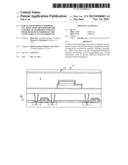
[0011] Referring now to FIG. 1, a planarized transistor 20 in conventionally formed. On top of the planarized surface of the transistor 20 is a ferroelectric capacitor including a bottom electrode (BE) 1, a ferroelectric layer 2, a top electrode (TE) 3. The ferroelectric capacitor is encapsulated using layers 4 as is known in the art. After the ferroelectric capacitor is formed, a ferroelectric oxide (FEO) is formed over the encapsulated ferroelectric capacitor and planarized.
[0012] PC referred to in the drawing figures is Poly silicide gate Contact, or simply poly contact.
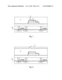
[0013] Referring now to FIG. 2, an FEO encapsulation layer 6 is formed, and a separation layer 7 is also formed.
[0014] The separation layer is used to prevent the reaction between the FEO encapsulation and Metal 1 (M1) layers. Suitable materials for this layer are described above.
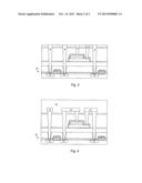
[0015] Referring now to FIG. 3, CMOS contacts 8 are formed through the FEO layer 5, the FEO encapsulation layer 6, and the separation layer 7 to the source and drain of the transistor 20, and to the bottom and top electrodes 1 and 3 of the ferroelectric capacitor. After the contacts are formed, the TEC recovery anneal is performed as described above.
[0016] Referring now to FIG. 4, Metal 1 (M1) 11 is formed, which in order of appearance from left to right metalizes the bit line, the intercell connection between the access transistor 20 and the ferroelectric capacitor, and the plate line. An interlayer dielectric layer 12 is then formed on top of the entire structure.
[0017] According to the present invention, an additional encapsulation layer and method is presented for additional protection against hydrogen degradation so that manufacturing yields can be improved.
[0018] It will be apparent to those skilled in the art, therefore, that various modifications and variations can be made to the invention without departing from the spirit or scope of the invention. Thus, it is intended that the present invention covers the modifications and variations of this invention provided they come within the scope of the appended claims.
User Contributions:
Comment about this patent or add new information about this topic:
| People who visited this patent also read: | |
| Patent application number | Title |
|---|---|
| 20170186623 | METHOD FOR PRODUCING LOW-PERMITTIVITY SPACERS |
| 20170186622 | SPACER-DAMAGE-FREE ETCHING |
| 20170186621 | METHOD OF ATOMIC LAYER ETCHING USING FUNCTIONAL GROUP-CONTAINING FLUOROCARBON |
| 20170186620 | SUBSTRATE PROCESSING METHOD AND SUBSTRATE PROCESSING SYSTEM |
| 20170186619 | ETCHING METHOD |
Images included with this patent application:
 |  |
 |
| New patent applications in this class: | |
| Date | Title |
|---|---|
| 2019-05-16 | Semiconductor device |
| 2016-06-23 | Compositions and methods for semiconductor processing and devices formed therefrom |
| 2016-05-26 | Composition for encapsulation film, encapsulation film, and electronic device comprising the same (as amended) |
| 2016-05-05 | Printed circuit module having a semiconductor device with a protective layer in place of a low-resistivity handle layer |
| 2015-11-12 | Semiconductor package |
| Top Inventors for class "Active solid-state devices (e.g., transistors, solid-state diodes)" | |
| Rank | Inventor's name |
|---|---|
| 1 | Shunpei Yamazaki |
| 2 | Shunpei Yamazaki |
| 3 | Kangguo Cheng |
| 4 | Huilong Zhu |
| 5 | Chen-Hua Yu |