Patent application title: POWER SWITCH CIRCUIT
Inventors:
Fu-Li Gao (Shenzhen City, CN)
Hsing-Suang Kao (Tu-Cheng, TW)
Hsing-Suang Kao (Tu-Cheng, TW)
Assignees:
HON HAI PRECISION INDUSTRY CO., LTD.
HONG FU JIN PRECISION INDUSTRY (ShenZhen) CO., LTD.
IPC8 Class: AH03K17687FI
USPC Class:
327427
Class name: Gating (i.e., switching input to output) utilizing three or more electrode solid-state device field-effect transistor
Publication date: 2013-09-19
Patent application number: 20130241627
Abstract:
A power switch circuit includes a pulse width modulation (PWM) control
circuit having a first frequency control terminal and a second frequency
control terminal for outputting predetermined frequency signals, a first
switch circuit, a second switch circuit, a first resistor connected
between the first frequency control terminal and the first switch
circuit, a second resistor connected between the first frequency control
terminal and the second switch circuit, a first filtering circuit having
a third resistor and a first capacitor, and a second filtering circuit
having a fourth resistor and a second capacitor. A first terminal of the
first capacitor is connected to the first switch circuit and a second
terminal of the first capacitor is grounded via the third resistor. A
first terminal of the second capacitor is connected to the second switch
circuit and a second terminal of the second capacitor is grounded via the
fourth resistor.Claims:
1. A power switch circuit, comprising: a pulse width modulation (PWM)
control circuit comprising a first frequency control terminal and a
second frequency control terminal for outputting predetermined frequency
signals; a first switch circuit; a second switch circuit; a first
resistor connected between the first frequency control terminal and the
first switch circuit; a second resistor connected between the first
frequency control terminal and the second switch circuit; a first
filtering circuit comprising a third resistor and a first capacitor,
wherein a first terminal of the first capacitor is connected to the first
switch circuit and a second terminal of the first capacitor is grounded
via the third resistor; and a second filtering circuit comprising a
fourth resistor and a second capacitor, wherein a first terminal of the
second capacitor is connected to the second switch circuit and a second
terminal of the second capacitor is grounded via the fourth resistor.
2. The power switch circuit as claimed in claim 1, wherein the first switch circuit comprises a first field effect transistor, and the second switch circuit comprises a second field effect transistor.
3. The power switch circuit as claimed in claim 2, wherein the second terminal of the first resistor is connected to the grid of the first field effect transistor, and the second terminal of the second resistor is connected to the grid of the second field effect transistor.
4. The power switch circuit as claimed in claim 2, wherein the first terminal of the first capacitor is connected to the source of the first field effect transistor, and the first terminal of the second capacitor is connected to the source of the second field effect transistor.
Description:
BACKGROUND
[0001] 1. Technical Field
[0002] The present disclosure relates to power switch circuits and, particularly, to a power switch circuit capable of reducing electromagnetic interference (EMI).
[0003] 2. Description of the Related Art
[0004] EMI effects performance of electronic devices greatly. For example, when power is supplied to a power switch circuit in an electronic device, power system harmonics may be created at the moment that a switch element of the power switch circuit is turned on causing EMI.
BRIEF DESCRIPTION OF THE DRAWING
[0005] The components in the drawing is not necessarily drawn to scale, the emphasis instead being placed upon clearly illustrating the principles of the disclosure. Moreover, in the drawing, like reference numerals designate corresponding parts throughout the several views.
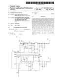
[0006] The FIGURE is a circuit diagram of a power switch circuit in accordance with an exemplary embodiment.
DETAILED DESCRIPTION
[0007] Referring to the FIGURE, a power switch circuit 10 includes a pulse-width modulation (PWM) control circuit 11, a first resistor R1, a second resistor R2, a first switch circuit 12, and a second switch circuit 13. The PWM control circuit 11 includes a first frequency control terminal DR1 and a second frequency control terminal DR2 configured for outputting predetermined frequency signals. A first terminal of the first resistor R1 is connected to the first frequency control terminal DR1, and a second terminal of the first resistor R1 is connected to the first switch circuit 12. A first terminal of the second resistor R2 is connected to the second frequency control terminal DR2, and a second terminal of the second resistor R2 is connected to the second switch circuit 13.
[0008] In the embodiment, the first switch circuit 12 includes a field effect transistor Q1, and the second switch circuit 13 includes a field effect transistor Q2. The second terminal of the first resistor R1 is connected to the grid of the field effect transistor Q1, the second terminal of the second resistor R2 is connected to the grid of the field effect transistor Q2. The drains of the field effect transistor Q1 and the field effect transistor Q2 are both connected to a power input port DC_IN.
[0009] The power switch circuit 10 further includes a first filtering circuit 14 and a second filtering circuit 15. The first filtering circuit 14 is connected between the first switch circuit 12 and a first output port 16 of the power switch circuit 10, and the second filtering circuit 15 is connected between the second switch circuit 13 and a second output port 17 of the power switch circuit 10. In the embodiment, the first filtering circuit 14 includes a third resistor R3 and a first capacitor C1. A first terminal of the first capacitor C1 is connected to the source of the field effect transistor Q1, and a second terminal of the first capacitor C1 is grounded via the third resistor R3. The second filtering circuit 15 includes a fourth resistor R4 and a second capacitor C2. A first terminal of the second capacitor C2 is connected to source of the field effect transistor Q2, and a second terminal of the second capacitor C2 is grounded via the fourth resistor R4.
[0010] In the embodiment, the PWM control circuit 11 is an integration circuit, and further includes a first feedback port FB1 grounded via a resistor R5 and a second feedback port FB2 grounded via a resistor R6. The first frequency control terminal DR1 is connected to the grid of the field effect transistor Q1, and the second frequency control terminal DR2 is connected to the grid of the field effect transistor Q2.
[0011] When the first frequency control terminal DR1 and the second frequency control terminal DR2 respectively output higher harmonics generated by the PWM control circuit 11, the first filtering circuit 14 and the second filtering circuit 15 are capable of restricting amplitude of the higher harmonics, thereby reducing electromagnetic interference of the power switch circuit 10.
[0012] In the embodiment, the power switch circuit 10 further includes other elements which are not related to the present disclosure and left out.
[0013] It is understood that the present disclosure may be embodied in other forms without departing from the spirit thereof. Thus, the present examples and embodiments are to be considered in all respects as illustrative and not restrictive, and the disclosure is not to be limited to the details given herein.
User Contributions:
Comment about this patent or add new information about this topic:
Images included with this patent application:
 |  |
| Similar patent applications: | |
| Date | Title |
|---|---|
| 2011-03-24 | Power switch circuit |
| 2011-09-29 | Power switch circuit |
| 2011-12-08 | Power switch circuit |
| 2012-08-16 | Polarity switch circuit for charger |
| 2009-10-01 | Power noise immunity circuit |
| New patent applications in this class: | |
| Date | Title |
|---|---|
| 2016-07-14 | Protected switching element |
| 2016-06-23 | Semiconductor device and semiconductor system |
| 2016-05-12 | Output discharge techniques for load switches |
| 2016-05-12 | Apparatus and methods for reducing charge injection mismatch in electronic circuits |
| 2016-04-28 | Methods and circuits for improved reliability of power devices operating under repetitive thermal stress |
| New patent applications from these inventors: | |
| Date | Title |
|---|---|
| 2013-10-31 | Tuner circuit |
| 2013-10-17 | Key detection circuit |
| 2013-10-17 | Signal processing circuit |
| 2013-10-10 | Anti-pop circuit |
| 2013-10-03 | Overvoltage protection circuit and electronic device |
| Top Inventors for class "Miscellaneous active electrical nonlinear devices, circuits, and systems" | |
| Rank | Inventor's name |
|---|---|
| 1 | Yantao Ma |
| 2 | Feng Lin |
| 3 | Ming-Chieh Huang |
| 4 | Yong-Ju Kim |
| 5 | Chan-Hong Chern |