Patent application title: MEMS ACTUATOR DEVICE WITH INTEGRATED TEMPERATURE SENSORS
Inventors:
Niladri Sarkar (Waterloo, CA)
Icspi Corp (Waterloo, CA)
Assignees:
ICSPI CORP.
IPC8 Class: AH02N1000FI
USPC Class:
318117
Class name: Electricity: motive power systems nonmagnetic motor thermoelectric motor
Publication date: 2013-07-11
Patent application number: 20130175952
Abstract:
An electro-thermal actuator which includes a unit cell comprising at
least one thermal bimorph, the thermal bimorph comprising at least two
materials of different thermal expansion coefficient bonded together, the
unit cell having a first end and a second end; and at least one
temperature sensor located on the at least one thermal bimorph for
measuring a temperature of the at least one thermal bimorph and
determining a position of the unit cell. The basic structure can be
expanded to 1-D, 2-D and 3-D positioners. The bimorphs can also be
coupled to an active yoke which is in turn anchored to a plate, in order
to reduce the parasitic heat effects on displacement of the tip of the
bimorph.Claims:
1-22. (canceled)
23. An electro-thermal actuator for positioning a element relative to a substrate, the electro-thermal actuator including a first actuator having a first end point and a second end point that is movable relative to the first end point, the first actuator comprising: a first unit cell having a first end and a second end, the first unit cell comprising a first thermal bimorph; a first heater that is operative to provide a first heat flow to the first unit cell; and a first temperature sensor that is operative for measuring a first temperature at a first location, wherein the first temperature is based on a second heat flow between the first unit cell and a second location that is external to the first unit cell; wherein the position of the second end relative to the first end is based on the first temperature and the first heat flow, and wherein the first actuator is operative for inducing motion of the element along a first direction.
24. The electro-thermal actuator of claim 23, wherein the first unit cell further comprises a second thermal bimorph, the first thermal bimorph and second thermal bimorph being physically coupled in series between the first end and the second end, and the second thermal bimorph being operative for mitigating development of a bending moment at one of the first end and second end, wherein the first thermal bimorph and second thermal bimorph are physically connected such that the first heater is operative to further provide the first heat flow to the second unit cell.
25. The electro-thermal actuator of claim 23, the first actuator further comprising a second temperature sensor that is operative for measuring a second temperature at a third location, wherein the first temperature sensor is located proximate the first end and the second temperature sensor is located proximate the second end; wherein the position of the second end relative to the first end is further based on the second temperature.
26. The electro-thermal actuator of claim 25, wherein each of the first location and third location is external to the first unit cell.
27. The electro-thermal actuator of claim 23, wherein the first location is external to the first unit cell.
28. The electro-thermal actuator of claim 23, further comprising a second actuator having a third end point and a fourth end point that is movable relative to the third end point, the second actuator comprising: a second unit cell comprising a second thermal bimorph; and a second heater that is operative to provide a third heat flow to the second unit cell; wherein the first actuator and second actuator are physically coupled such that the motion of the element is based on the first heat flow, the second heat flow, and the third heat flow, and wherein the second heat flow is based on the third heat flow.
29. The electro-thermal actuator of claim 28, wherein the second actuator is operative for moving the element along a second direction that is orthogonal to the first direction.
30. The electro-thermal actuator of claim 23, wherein the substrate comprises the second location.
31. The electro-thermal actuator of claim 23, the first actuator further comprising a second unit cell having a second thermal bimorph, a third end, and a fourth end, the first unit cell and second unit cell being physically coupled in parallel such that (1) the first end and third end are physically connected at the first end point and collectively define a first plane and (2) the second end and fourth end are physically connected at the second end point.
32. The electro-thermal actuator of claim 31, wherein first actuator is dimensioned and arranged such that the first direction is substantially within the first plane.
33. The electro-thermal actuator of claim 31, wherein first actuator is dimensioned and arranged such that the first direction is substantially orthogonal to the first plane.
34. The electro-thermal actuator of claim 31, further comprising an active yoke for physically coupling the first unit cell and second unit cell at one of the first end point and the second end point, the active yoke comprising a third thermal bimorph that has a length shorter than each of the first thermal bimorph and the second thermal bimorph.
35. The electro-thermal actuator of claim 23, further including a second actuator having a third end point and a fourth end point that is movable with respect to the third end point, the second actuator comprising: a second unit cell comprising a second thermal bimorph; a second heater that is operative to provide a third heat flow to the second unit cell; and a second temperature sensor that is operative for measuring a second temperature at a third location, wherein the second temperature is based on a fourth heat flow between the second unit cell and a fourth location that is external to the second unit cell; wherein the position of the fourth end point relative to third end point is based on the second temperature and the fourth heat flow, and wherein the second actuator is operative for moving the element along a second direction that is unaligned with the first direction.
36. The electro-thermal actuator of claim 35, wherein the second direction and the first direction are substantially orthogonal.
37. The electro-thermal actuator of claim 35, further comprising a third actuator having a fifth end point and a sixth end point that is movable along a third direction with respect to the fifth end point, the third actuator comprising: a third unit cell comprising a third thermal bimorph; a third heater that is operative to provide a fifth heat flow to the third unit cell; and a third temperature sensor that is operative for measuring a third temperature at a fifth location, wherein the third temperature is based on a sixth heat flow between the third unit cell and a sixth location that is external to the third unit cell; wherein the position of the sixth end relative to third end is based on the third temperature and the fifth heat flow, and wherein the third actuator is operative for moving the element along a third direction, and further wherein the first direction, second direction, and third direction are mutually orthogonal.
38. The electro-thermal actuator of claim 23 wherein the substrate defines a first plane, and wherein the element comprises: a first piezoresistor; and a second piezoresistor; wherein the first and second piezoresistors are arranged such that they are at substantially the same temperature, and wherein each of the first and second piezoresistor cantilevers from the second end such that the free end of the first piezoresistor projects further away from the first plane than the free end of the second piezoresistor when the first electro-thermal actuator is actuated.
39. An electro-thermal actuator for positioning a element relative to a substrate, the electro-thermal actuator comprising a first actuator operative for translating the element along a first direction, the first actuator comprising: a plurality of first unit cells physically coupled in parallel between a first end and a second end, each first unit cell comprising at least one thermal bimorph; a first heater that is operative to provide a first heat flow to the first actuator; and a first temperature sensor that is operative for measuring a first temperature at a first location, wherein the first temperature is based on a second heat flow between the plurality of first unit cells and a second location that is external to the plurality of first unit cells; wherein the position of the element along the first direction is based on the first temperature and the first heat flow.
40. The electro-thermal actuator of claim 39, further comprising an active yoke for coupling at least one first unit cell of the plurality of first unit cells at one of the first end and the second end, the active yoke comprising a thermal bimorph having a shorter length than the thermal bimorph of the at least one first unit cell.
41. The electro-thermal actuator of claim 39, further comprising a second actuator operative for translating the element along a second direction that is substantially orthogonal to the first direction, the second actuator comprising: a plurality of second unit cells physically coupled in parallel between a third end and a fourth end, each second unit cell comprising at least one thermal bimorph; a second heater that is operative to provide a third heat flow to the second actuator; and a second temperature sensor that is operative for measuring a second temperature at a third location, wherein the second temperature is based on a fourth heat flow between the plurality of second unit cells and a fourth location that is external to the plurality of second unit cells; wherein the position of the element along the second direction is based on the second temperature and the third heat flow.
42. The electro-thermal actuator of claim 41, further comprising a third actuator operative for translating the element along a third direction, the first direction, second direction, and third direction being substantially mutually orthogonal, and the third actuator comprising: a plurality of third unit cells physically coupled in parallel between a fifth end and a sixth end, each third unit cell comprising at least one thermal bimorph; a third heater that is operative to provide a fifth heat flow to the third actuator; and a third temperature sensor that is operative for measuring a third temperature at a fifth location, wherein the third temperature is based on a sixth heat flow between the plurality of third unit cells and a sixth location that is external to the plurality of third unit cells; wherein the position of the element along the third direction is based on the third temperature and the sixth heat flow.
43. A method for positioning a element relative to a substrate, the method comprising: providing a first heat flow to a first actuator that includes a first thermal bimorph, wherein the first actuator is operative for positioning the element along a first direction; determining a second heat flow between the first actuator and a first location that is external to the first thermal bimorph; and controlling the first heat flow based on the second heat flow.
44. The method of claim 43 wherein the second heat flow is determined by operations comprising: measuring a first temperature at a first location that is external to the first actuator; measuring a second temperature at a second location that is external to the first actuator, wherein the first location and second location are separated by a known thermal resistance path; and computing a value for the second heat flow based on the first temperature and the second temperature.
45. The method of claim 43 further comprising: providing a third heat flow to a second actuator that includes a second thermal bimorph, wherein the second actuator is operative for positioning the element along a second direction that is unaligned with the first direction; determining a fourth heat flow between the second actuator and a second location that is external to the second thermal bimorph; and controlling the third heat flow based on the fourth heat flow.
46. The method of claim 45 further comprising: providing a fifth heat flow to a third actuator that includes a third thermal bimorph, wherein the third actuator is operative for positioning the element along a third direction, and wherein the first direction, second direction, and third direction are substantially mutually orthogonal; determining a sixth heat flow between the third actuator and a third location that is external to the third thermal bimorph; and controlling the fifth heat flow based on the sixth heat flow.
47. The method of claim 43 further comprising: providing the first actuator such that it further comprises a second thermal bimorph, wherein the first thermal bimorph and second thermal bimorph are coupled in series between a first end point and a second end point, and wherein the second thermal bimorph is shorter than the first thermal bimorph, and further wherein the second thermal bimorph and first thermal bimorph are arranged such that the development of a bending moment at one of the first end and second end is mitigated.
Description:
FIELD OF THE INVENTION
[0001] The present invention is in general related to nanopositioning and to CMOS-MEMS (Complementary Metal Oxide Semiconductor--Micro-electromechanical System) devices capable of positioning a payload with sub-nanometer resolution in a closed-loop fashion. More particularly, it relates to thermal bimorph actuators having integrated temperature sensors for mitigating thermal coupling effects.
BACKGROUND OF THE INVENTION
[0002] The fabrication of features with dimensions of several hundreds of atoms has become quite routine in semiconductor manufacturing. However, conventional fabrication, inspection, and metrology tools are being stretched to their limits.
[0003] Atomically precise metrology tool requirements include enhanced resolution, stability and throughput as well as scaled-up array operation and ultra-high vacuum (UHV) compatibility. Another requirement is nano-scale closed-loop position control in all three degrees of freedom.
[0004] Scanning probe microscopy covers several related technologies for imaging and measuring surfaces on a fine scale, down to atomic resolution. A scanning probe microscope (SPM) scans an extremely sharp tip of a probe across an object surface while measuring the probe tip-sample interaction via a tunnelling current, atomic force, capacitance, work-function, near field optical detection, or some other means. The imaging signal associated with the scanning probe tip-sample interaction is provided to an imaging system for suitable processing and image rendering.
[0005] Conventional SPMs use piezoelectric materials to provide the necessary resolution for scanning. Piezoelectric materials change shape when an electric voltage is applied across them. However, it takes a relatively high voltage--about 100 volts--to make a piezoelectric actuator change shape. This makes for expensive control electronics. In addition, these materials exhibit creep, which compromises the ability to position the probe tip deterministically and with a high degree of stability. With conventional SPMs, the mechanical path between the tip and the sample is sensitive to small temperature variations causing relatively large drift, and is also inherently less mechanically stable than for a miniaturized device. Moreover, it is difficult to implement array architectures using a conventional SPMs.
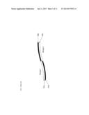
[0006] Fine-scale MEMS (micro-electromechanical systems) positioners provide an alternative to piezoelectric actuators. MEMS-based metrology devices are generally less expensive to manufacture. The driving electronics can be less expensive, since less voltage is required for some types of actuation. However, many MEMS positioners have no electrical signal routing, no position feedback, no integration of sensors inside the actuator, and limited resolution.
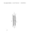
[0007] Examples of Static Position Sensing in MEMS include:
[0008] 1) capacitive sensing (charge sensing), where the voltage signal is low and susceptible to noise;
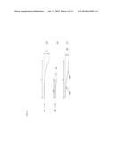
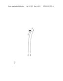
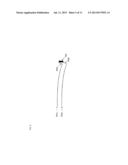
[0009] 2) piezoresistive sensing, which requires careful thermal balancing and has limitations on ultimate resolution; and
[0010] 3) optical sensing, which requires tedious alignment and is not amenable to array architectures.
[0011] Dynamic position sensing can make use of lock-in amplifier techniques.
[0012] A SPM implemented in a CMOS-MEMS process is described in "A CMOS-MEMS Scanning Probe Microscope with Integrated Position Sensors", Niladri Sarkar et al. The CMOS-MEMS SPM, with actuators arranged around a central stage that houses a cantilevered probe, allows the integration of all the critical actuation, sensing, and electronic components of an SPM on a wafer that can be batch fabricated in a conventional foundry thereby reducing the size and cost of the SPM while providing the required sensitivity and resolution. However, a main source of disturbance in the position control of the CMOS-MEMS SPM is unwanted parasitic thermal coupling between the actuators and the wafer substrate.
[0013] Therefore, there is a need for a MEMS nanopositioner design that provides high resolution and sensitivity while mitigating the problems of thermal coupling.
SUMMARY OF THE INVENTION
[0014] In accordance with one aspect of the present invention, there is provided an electro-thermal actuator which includes:
[0015] a unit cell comprising at least one thermal bimorph, the thermal bimorph comprising at least two materials of different thermal expansion coefficient bonded together, the unit cell having a first end and a second end; and
[0016] at least one temperature sensor located on the at least one thermal bimorph for measuring a temperature of the at least one thermal bimorph and determining a position of the unit cell.
[0017] In accordance with another aspect of the present invention, there is provided a one-dimensional positioner for positioning a stage. The one-dimensional positioner includes:
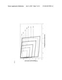
[0018] an electrothermal actuator for translating the stage essentially in one direction, the electrothermal actuator comprising:
[0019] a unit cell comprising at least one thermal bimorph, the thermal bimorph comprising at least two materials of different thermal expansion coefficient bonded together, the unit cell having a first end and a second end; and
[0020] at least one temperature sensor located on the at least one thermal bimorph for measuring a temperature of the at least one thermal bimorph and determining a position of the unit cell; and
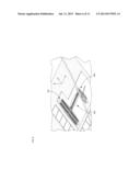
[0021] wherein the electrothermal actuator is mechanically coupled to the stage.
[0022] In accordance with another aspect, there is provided a two-dimensional positioner for positioning a stage. The two-dimensional positioner includes:
[0023] a pair of electrothermal actuators, each electrothermal actuator comprising:
[0024] a unit cell comprising at least one thermal bimorph, the thermal bimorph comprising at least two materials of different thermal expansion coefficient bonded together, the unit cell having a first end and a second end; and
[0025] at least one temperature sensor located on the at least one thermal bimorph for measuring a temperature of the at least one thermal bimorph and determining a position of the unit cell; and
[0026] the pair of electrothermal actuators arranged orthogonally such that a first one of the pair of electrothermal actuators translates the stage in a first direction and a second one of the pair of electrothermal actuators translates the stage in a second direction orthogonal to the first direction.
[0027] In accordance with yet another aspect of the invention, there is provided a three-dimensional positioner for positioning a stage. The three-dimensional positioner includes:
[0028] three electrothermal actuators, each electrothermal actuator including:
[0029] a unit cell comprising at least one thermal bimorph, the thermal bimorph comprising at least two materials of different thermal expansion coefficient bonded together, the unit cell having a first end and a second end; and
[0030] at least one temperature sensor located on the at least one thermal bimorph for measuring a temperature of the at least one thermal bimorph and determining a position of the unit cell; and
[0031] the electrothermal actuators arranged mutually orthogonally such that a first one of the electrothermal actuators translates the stage in a first direction, a second one of the electrothermal actuators translates the stage in a second direction orthogonal to the first direction, and a third one of the electothermal actuators translates the stage in a third direction orthogonal to the first direction and the second direction.
[0032] In accordance with still another aspect of the invention, there is provided an active yoke to couple multiple actuators together while increasing force and stiffness and retaining optimal stroke. The active yoke is a bimorph of a shorter length and narrower cross section that provides equal and opposite tip rotation in order to cancel the angular deflection of the actuator tip. A plate can thus be used to couple all the actuators together without loss of deflection. Without such a yoke, coupling the actuators to a plate would impose a zero-moment constraint at the tip of the actuator beams, resulting in zero deflection. The conventional method to mitigate this issue is to employ a pair of symmetrically opposed bimorphs to cancel the tip rotation; however, the proposed method has been shown to produce ˜75% more deflection than the state-of-the-art.
[0033] Still another aspect of the invention provides a pair of thermally balanced piezoresistive sensors that can be used to measure externally applied forces, or augment the position resolution of the actuator. The balanced pair of piezoresistors is arranged differentially with respect to strain, such that upon the actuator's lateral deflection, one experiences compressive strain while the other experiences tensile strain. Similar arrangements can be used for out-of-plane measurements.
[0034] In accordance with another embodiment, the piezoresistors may be arranged in an opposed pair of cantilevers such that both piezoresistors are at the same o temperature but only one interacts with the sample.
[0035] In accordance with yet another aspect of the invention, there is provided a method of singulating the devices from a single wafer, obviating the need for a backside deep reactive ion etch (DRIE) step. The convention DRIE method requires a lithography and patterning step that is both time consuming and expensive. The proposed method employs a conventional wafer saw to dice grooves in the backside of the wafer, such that upon release of the device layer, the chips are singulated once the top-side etch reaches the backside groove,
[0036] In accordance with yet another aspect of the invention, there is provided a method of obtaining multiple sharp tips in a common work area with spacings that are not achievable using conventional lithography. The method employs a design pattern in which all positioners are coupled to a plate at their distal ends. The focused ion beam (FIB) instrument is then used to mill sub-micron grooves that define various arrangements, geometry and spacing of the tips as specified by the operator.
[0037] Each actuator may act as a 1-D positioner.
[0038] In accordance with another aspect of the invention there is provided a 2-D system based on orthogonally arranged thermal bimorph actuators.
[0039] In accordance with another aspect of the invention there is provided a 2-D system based on a flexured arrangement of thermal bimorph actuators.
[0040] In accordance with another aspect of the invention there is provided a 3-D system based on a combination of flexured arrangements and orthogonal arrangements of thermal bimorph actuators.
[0041] It will be appreciated by the reader that the method described herein can also be used with chevron-type actuators that consist of a single material, among other actuators. In fact, most electro-thermal actuators can make use of these techniques.
[0042] Other features and advantages of the present invention will be better understood upon reading of preferred embodiments thereof with reference to the appended drawings.
BRIEF DESCRIPTION OF THE DRAWINGS
[0043] For a better understanding of the invention and to show how the same may be carried into effect, reference is now made by way of example to the accompanying drawings in which:
[0044] FIG. 1 is a representation of a unit cell consisting of a pair of symmetrically opposed bimorphs;
[0045] FIG. 2 is a representation of a set of unit cells (coupled in parallel) mirrored about the axis of symmetry in order to eliminate parasitic out-of-plane motion;
[0046] FIG. 3 is a graph showing the comparison of the deflection obtained with various arrangements of bimorphs;
[0047] FIG. 4 is a representation of 2 bimorphs coupled together to a plate using conventional yokes;
[0048] FIG. 5 is a representation of 2 bimorphs coupled together to a plate using active yokes;
[0049] FIG. 6 is a schematic representation of an XYZ positioner that suffers from parasitic thermal coupling;
[0050] FIG. 7 is a graph showing the data taken on an XY positioner operating under open-loop conditions;
[0051] FIG. 8 is a schematic representation of a CMOS-MEMS scanning probe microscope with integrated actuation and sensing;
[0052] FIG. 9 is a schematic representation of a differential arrangement of piezoresistors in a pair of symmetrically opposed bimorphs;
[0053] FIG. 10 is a schematic representation of the method to singulate scanning probe microscope devices fabricated on a single starting wafer; and
[0054] FIG. 11 is a schematic representation of a method for create tips using a focused ion beam (FIB) instrument.
DESCRIPTION OF THE INVENTION
[0055] The present invention is directed to a system and method which is operable to manipulate a sharp probe with sub-nanometer position resolution in x, y and z coordinates in a closed-loop fashion.
[0056] Actuation is achieved using the thermal bimorph effect. This effect relies on a mismatch in thermal expansion coefficients between two materials in a monolithic beam structure, in order to achieve a deflection as a function of temperature. Lateral actuation is achieved by offsetting the internal metal layers in the beam, thus resulting in bimorph layers encased in the monolithic beam.
[0057] Reducing the width of the beam increases the deflection. However, a single thin beam does not provide high forces and large out-of-plane stiffness (required in is AFM, STM, probing applications). The output force and out-of-plane stiffness can be increased by coupling several of these bimorphs together. This is made possible through the use of symmetrically opposed bimorphs in order to cancel the rotation at the tips.
[0058] Referring now to FIG. 1, there is shown a unit cell consisting of a pair of symmetrically opposed bimorphs. In their simplest expression, bimorphs consist of a pair of materials which have different coefficients of thermal expansion. In FIG. 1, there are show two bimorphs 1, 2 which are symmetrically opposed (i.e. materials on bimorph is on the bottom, whereas on bimorph, it is on top). Bimorph 1 consists of material 101a and 101b, whereas bimorph 2 consists of materials 102b and 102a.
[0059] Referring now to FIG. 2, there is shown several unit cells coupled in parallel 202a, 202b and mirrored about the axis of symmetry 201 in order to eliminate parasitic out-of-plane motion.
[0060] The state of the art for a single actuator is represented in the figure above. The shortcoming of this approach is that displacement is reduced by a factor of two in order to cancel out the rotation at the tip.
[0061] In FIG. 3(a) there is shown a bimorph of length L that achieves a deflection d upon heating. The second case shown in FIG. 3(b) is a beam of length L/2 that achieves a displacement of d/4, due to the (d α L2) relationship. The third case shown in FIG. 3(c) illustrates the unit cell consisting of two opposed bimorphs having a length L that achieves d/2 displacement.
[0062] An alternate approach to coupling several bimorphs together is to use a yoke (mechanical flexure) to couple the bimorphs together.
[0063] More specifically, in FIG. 2, the beams (there are 7 of them) are arranged in the symmetrically opposed fashion described in 303a and 303b. This arrangement enables direct coupling to a plate, since there is no rotation at the tip of a single beam when it is free at the distal end. This arrangement, however, only achieves 1/2 of the deflection of the bimorph beam in 301. In FIG. 4, instead of using the bimorph arrangement in 303a/b, we use a single bimorph beam as shown in FIG. 301. Two of these beams are coupled to a plate using "yoke" flexures that are not bimorphs. The force required to bend this passive yoke flexures detracts from the overall deflection of the bimorph beams. In FIG. 5, the yokes are mini-bimorphs that oppose the tip rotation of the actuator bimorphs, so that they can be coupled to a plate without loss of deflection.
[0064] The yoke approach results in less overall displacement than the opposed bimorphs approach in FIG. 3c. This is because the strain energy required to bend the yokes reduces the amount of mechanical work that the actuators can perform. One aspect of the present invention improves the overall actuation achievable by coupled actuators with the introduction of an "active yoke" as shown in FIG. 5.
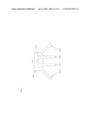
[0065] The active yoke according to the present invention is a short bimorph 502a, 502b that is coupled to plate 503 that bends in order to counter the moment at the tip of the actuator bimorph--this reduces the amount of work that is lost to bending energy. The overall displacement that is achieved by this configuration, when the yoke is properly designed, can be increased by >60%.
[0066] Passive yokes (FIG. 4) have been used in the past, but active yokes (FIG. 5) are novel. The structural difference between FIGS. 4 and 5 is the addition of the is bimorph in the yokes of FIG. 5, which turns them into bimorphs. The functional difference between the figures is that the yokes in FIG. 5 deflect upon heating, and they are designed to exactly cancel out the angular rotation at the tip of the actuator bimorphs, resulting in the zero-moment condition referred to.
[0067] The main source of disturbance in the position control system for the nanopositioner is thermal coupling. This is shown in FIG. 6 (ref: US patent application publication no. 2007/0278896) in which all three axes are mechanically, electrically, and thermally coupled.
[0068] In this Figure, when the z-actuator 603 is powered and reaches a steady-state temperature, heat flows through the x-actuator 602 and the y-actuator 604 to the substrate (at ambient temperature) to maintain thermal equilibrium.
[0069] The parasitic heat flow through the x and y actuators results in an undesired deflection of the actuators. This is suppressed using distributed temperature sensors that measure the temperature of the electro-thermal actuators at various locations in order to calculate their position. Polysilicon resistors that are used in this process have a temperature coefficient of resistivity that is sufficiently high for accurate thermal measurements. The heat flowing into/out of the positioners from mechanically coupled actuators or into a substrate (at ambient temperature) can be deduced from a pair of temperature measurements on either end of a known thermal resistance path. A control system with temperature inputs and position outputs can be used to control position with sub-nanometer precision.
[0070] Another drawback of thermal coupling is that the devices have a limited range of motion corresponding to their rest position while neighboring actuators are at max power (significantly offset from the power-off rest position).
[0071] FIG. 7 shows the data taken on an XY positioner operating under open-loop conditions.
[0072] The driving signals are intended to move the payload in a rectilinear fashion; however due to thermal coupling effects, parasitic motion in the orthogonal axis accompanies the desired motion. Concentric paths 701a-f represent incrementally increasing driving voltages. Bounding box 702 represents the region of operation in which closed-loop control can eliminate coupling effects.
[0073] In order to mitigate the effects of thermal coupling and increase the useful range of motion of these devices, thermal shunt paths can be used to redirect heat to the substrate instead of to other actuators. In addition, temperature sensors can be placed at either end of these thermal shunt paths in order to quantify the heat flow and use it as an input to the control system.
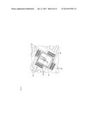
[0074] FIG. 8 shows a CMOS-MEMS scanning probe microscope with integrated actuation and sensing. Lateral actuators (801) are arranged orthogonally to balance torques on the center stage that houses the z-actuator (804) and balanced cantilevers (803). Flexures (802) are used to couple the lateral actuators to the central stage. Temperature sensors (805) are placed strategically to measure the direction of heat flow and average temperature of the actuators for an accurate estimate of position.
[0075] Decoupled and orthogonal motion in the 3 axes is desirable. An additional method to of reducing the thermal coupling is to use high thermal resistance materials to mechanically couple parts of the device together, while isolating them thermally.
[0076] To measure external forces exerted onto the positioner, a thermally balanced pair of piezoresistors can be used to compare desired deflection to actual deflection. In this implementation, a lookup table may be used for comparison of expected vs. measured values.
[0077] This is illustrated in FIG. 9, which Illustrates a differential arrangement of piezoresistors (901, 902) in a pair of symmetrically opposed bimorphs (903a, 903b). One piezoresistor is in compressive strain (901) while the other is in tensile strain (902), and both are at the same temperature.
[0078] To operate these 3 DOF positioners over a sample we can remove a portion of the substrate underneath the distal end of the devices using a back-side etch process This process is difficult to implement on a wafer scale due to non-uniformities in the etch rate. It is also costly and time consuming since it requires a patterning step followed by an extended period of time in a Deep Reactive Ion Etch instrument. Thus, another aspect of the invention is to use a dicing saw to cut grooves in the backside of the wafer and then perform a standard device release process from the top side.
[0079] In FIG. 10, Illustration of method to singulate scanning probe microscope devices fabricated on a single starting wafer (1001). A backside groove (1002) is created using a dicing saw. In the final step (1003), reactive ions (1003c) are used to etch the device from the top side, yielding released cantilevers (1003a) and defining a new die edge (1003b).
[0080] Referring now to FIG. 11, there is schematically illustrated a method for creating type using a focused Ion Beam instrument. Beams from the positioner 1101 a-d terminate on a plate 103. The milling lines 1102 generated by the FIB are used to define tip geometry.
[0081] Of course, numerous modifications could be made to the embodiment described above without departing from the scope of the present invention.
User Contributions:
Comment about this patent or add new information about this topic:

