Patent application title: ADAPTIVE FREQUENCY COMPENSATION FOR PFC POWER CONVERTER OPERATING IN CCM AND DCM
Inventors:
Ta-Yung Yang (Taoyuan City, TW)
Ta-Yung Yang (Taoyuan City, TW)
Ying-Chi Chen (Taipei City, TW)
Chien-Tsun Hsu (Taipei City, TW)
Cheng-Sung Chen (Taichung City, TW)
Assignees:
SYSTEM GENERAL CORPORATION
IPC8 Class: AG05F170FI
USPC Class:
323205
Class name: Electricity: power supply or regulation systems for reactive power control
Publication date: 2013-06-06
Patent application number: 20130141056
Abstract:
A control circuit of a power factor correction (PFC) converter is
provided. The control circuit includes a pulse width modulation (PWM)
circuit, an amplifier, a detection circuit., and a capacitor. The PWM
circuit generates a switching signal in response to a loop signal. The
amplifier is coupled to generate the loop signal in response to a
switching current. The detection circuit generates a mode signal coupled
to change output impedance of the amplifier. The capacitor is coupled to
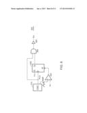
the amplifier for loop frequency compensation. The switching signal is
coupled to switch an inductor of the PFC power converter and generate the
switching current.Claims:
1. A control circuit of a power factor correction (PFC) converter
comprising: a pulse width modulation (PWM) circuit generating a switching
signal in response to a loop signal; an amplifier coupled to receive a
switching current for generating the loop signal; a detection circuit
generating a mode signal coupled to change output impedance of the
amplifier; and a capacitor coupled to the amplifier for loop frequency
compensation; wherein the switching signal is coupled to switch an
inductor of the PFC power converter and generate the switching current.
2. The circuit as claimed in claim 1, wherein the mode signal indicates a CCM (continuous current mode) or DCM (discontinuous current mode) operation.
3. The circuit as claimed in claim 1, wherein the mode signal is generated in response to an input voltage of the PFC power converter, an output voltage of the PFC power converter, and the switching signal.
4. The circuit as claimed in claim 1, wherein the amplifier is a transconductance amplifier.
5. The circuit as claimed in claim 1, wherein the mode signal is coupled to change a bias current of the amplifier.
6. The circuit as claimed in claim 1, wherein the loop signal is a current loop signal generated by comparing the switching current with a command signal.
7. The circuit as claimed in claim 6, wherein the command signal is generated
8. A method for controlling a power factor correction (PFC) converter comprising: generating a switching signal in response to a loop signal; generating the loop signal in accordance with a switching current; generating a mode signal coupled to change the impedance of the loop signal; compensating the loop signal with a capacitor; wherein the switching signal is coupled to switch an inductor of the PFC power converter and generate the switching current.
9. The method as claimed in claim 8, wherein the mode signal indicates a CCM (continuous current mode) or DCM (discontinuous current mode) operation.
10. The method as claimed in claim 8, wherein the mode signal is generated in response to an input voltage of the PFC power converter, an output voltage of the PFC power converter, and the switching signal.
11. The method as claimed in claim 8, wherein the loop signal is generated by a transconductance amplifier.
12. The method as claimed in claim 8, wherein the mode signal is coupled to change a bias current of the transconductance amplifier.
13. The method as claimed in claim 8, wherein the loop signal is a current loop signal generated by comparing the switching current with a command signal.
14. The method as claimed in claim 13, wherein the command signal is generated in response to an input voltage of the PFC power converter.
15. The method as claimed in claim 8, wherein the impedance associated with the loop signal and capacitance of the capacitor develop a low-pass filter for the loop signal.
Description:
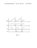
CROSS REFERENCE TO RELATED APPLICATIONS
[0001] This application claims the benefit of U.S. Provisional Application No. 61/565,543, filed on Dec. 1, 2011, the contents of which are incorporated herein by reference.
BACKGROUND OF THE INVENTION
[0002] 1. Field of the Invention
[0003] The invention relates to a control circuit, and more particularly to a control circuit of a PFC (power factor correction) power converter for adaptive frequency compensation of the FPC converter operating in a CCM (continuous current mode) and a DCM (discontinuous current mode).
[0004] 2. Description of the Related Art
[0005] In a conventional PFC (power factor correction) power converter, there is a current loop through an inductor. The loop gain of the current loop is different when the PFC power converter operates in a CCM (continuous current mode) and a DCM (discontinuous current mode). The loop gain is higher in the CCM operation. Thus, a lower bandwidth is required for achieving the loop stability of the current loop. However, the lower bandwidth's current loop results in a poor PF value.
[0006] Thus, it is desired to provide a control circuit of a PFC power converter, which provides improved frequency compensation for a current loop of the PFC power converter.
BRIEF SUMMARY OF THE INVENTION
[0007] An exemplary embodiment of a control circuit of a power factor correction (PFC) converter is provided. The control circuit comprises a pulse width modulation (PWM) circuit, an amplifier, a detection circuit, and a capacitor. The PWM circuit generates a switching signal in response to a loop signal. The amplifier is coupled to generate the loop signal in response to a switching current. The detection circuit generates a mode signal coupled to change output impedance of the amplifier. The capacitor is coupled to the amplifier for loop frequency compensation. The switching signal is coupled to switch an inductor of the PFC power converter and generate the switching current.
[0008] An exemplary embodiment of a method for controlling a power factor correction (PFC) converter is provided. The method comprises the steps of: generating a switching signal in response to a loop signal; generating the loop signal in accordance with a switching current; generating a mode signal coupled to change impedance associated with the loop signal; compensating for the loop frequency compensation of the PFC power converter with a capacitor. The switching signal is coupled to switch an inductor of the PFC power converter and generate the switching current.
[0009] A detailed description is given in the following embodiments with reference to the accompanying drawings.
BRIEF DESCRIPTION OF THE DRAWINGS
[0010] The invention can be more fully understood by reading the subsequent detailed description and examples with references made to the accompanying drawings, wherein:
[0011] FIG. 1 shows a PFC power converter;
[0012] FIG. 1A shows DCM waveforms of a switching signal, a switching current, and a switching current signal in FIG. 1;
[0013] FIG. 1B shows CCM waveforms of a switching signal, a switching current, and a switching current signal in FIG. 1;
[0014] FIG. 2 shows an exemplary embodiment of a control circuit of the PFC power converter in FIG. 1;
[0015] FIG. 3 shows an exemplary embodiment of a synthesis circuit of the control circuit in FIG. 2;
[0016] FIG. 4 shows an exemplary embodiment of an emulation circuit 170 of the synthesis circuit in FIG. 3;
[0017] FIG. 5 shows an exemplary embodiment of a detection circuit of the control circuit in FIG. 2;
[0018] FIG. 6 shows an exemplary embodiment of a PWM circuit of the control circuit in FIG. 2;
[0019] FIG. 7 shows waveforms of a ramp signal, a pulse signal, a switching signal, and a pulse of the control circuit in FIG. 2;
[0020] FIGS. 8 and 9 show equivalent circuits of a transconductance amplifier of the control circuit in FIG. 2; and
[0021] FIG. 10 shows waveforms of a switching-current command signal, a synthesis current signal, an equivalent voltage, and a current loop signal of the control circuit in FIG. 2.
DETAILED DESCRIPTION OF THE INVENTION
[0022] The following description is of the best-contemplated mode of carrying out the invention. This description is made for the purpose of illustrating the general principles of the invention and should not be taken in a limiting sense. The scope of the invention is best determined by reference to the appended claims.
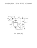
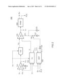
[0023] The present invention provides a method and apparatus for frequency compensation of a PFC (power factor correction) power converter operating in a CCM (continuous current mode) and a DCM (discontinuous current mode). FIG. 1 is a PFC power converter. Referring to FIG. 1, the PFC power converter comprises a resistor 35 connected to sample a switching current IL of an inductor 20 and generate a switching current signal VS coupled to a PFC control circuit 100. According to the switching current signal VS, the control circuit 100 will generate a switching signal SW to switch the inductor 20 and generate the switching current IL via a power transistor 30. Through the sensing of the switching current signal VS, the control circuit 100 generates the switching signal SW for producing the switching current IL. The switching current IL further generate the switching current signal VS at the resistor 35, which develops a current loop for PFC control. A capacitor 53 is used for the frequency compensation of the current loop. As described above, the loop gain of the current loop is different when the PFC power converter operates in the CCM or DCM. The loop gain is higher in the CCM operation. Thus, a lower bandwidth (higher capacitance of the capacitor 53) is required for achieving the loop stability of the current loop. However, the lower bandwidth's current loop results in a poor PF value. The object of this invention is to develop adaptive frequency compensation for the current loop to achieve a stable CCM operation and a good PF value for both CCM and DCM.
[0024] A resistor 50 is coupled to detect an input voltage VIN coupled to the inductor 20 and generate an input-voltage signal IAC coupled to the control circuit 100. The input voltage VIN is generated by a rectifier 10 according to an AC voltage VAC. The switching current IL of the inductor 20 is discharged to an output capacitor 45 via a rectifier 40 to generate an output voltage VO. Resistors 41 and 42 form a voltage divider coupled to the output of the PFC power converter to detect the output voltage VO and generate a signal VFB coupled to the control circuit 100 for the regulation of the output voltage VO. The signal VFB, the switching signal SW, and the output voltage VO develop a voltage loop for the PFC control. A capacitor 51 is used for the frequency compensation of the voltage loop.
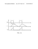
[0025] FIG. 1A shows the DCM waveforms of the switching signal SW, the switching current IL, and the switching current signal VS. The switching current IL of the inductor 20 is fully discharged before the start of the next switching cycle.
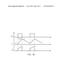
[0026] FIG. 1B shows the CCM waveforms of the switching signal SW, the switching current IL, and the switching current signal VS. The switching current IL of the inductor 20 still has a current I1 existed in the inductor 20 before the start of the next switching cycle. Therefore, the gain of the CCM is high.
L × i t = L × I A + I B T = L × 1 T × ( I 1 × T ON + V IN L × T ON ) ( 1 ) I L = 1 T × ( I 1 × T ON + V IN L × T ON ) ( 2 ) ∂ I L ∂ T ON = I 1 T + V IN T × L ( 3 ) V O = V IN + ( L × i t ) ( 4 ) V O = V IN + [ L × 1 T × ( I 1 × T ON + V IN L × T ON ) ] ( 5 ) ∂ V O ∂ T ON = I 1 × L T + V IN T ( 6 ) ##EQU00001##
[0027] wherein L is the inductance of the inductor 20; T is the switching period; TON is on time of the switching signal SW.
[0028] Equation (3) is the current loop gain (the switching current IL versus "the on time TON of the switching signal SW"). The continuous current I1 causes the higher current loop gain. Equation (6) is the voltage loop gain (the output voltage VO versus "the on time TON of the switching signal SW"). The continuous current I1 causes the higher voltage loop gain as well.
[0029] FIG. 2 is a preferred embodiment of the control circuit 100 according to the present invention. A transconductance amplifier (Gm) 110 is coupled to receive the signal VFB and a reference signal VR for generating a voltage loop signal VEA. The capacitor 51 is coupled to the voltage loop signal VEA (shown in FIG. 1) for the voltage loop compensation. A current source 115 provides a bias current Im for the transconductance amplifier 110. A multiplier-divider (M) 130 generates "a switching-current command signal VM" in accordance with the voltage loop signal VEA and the input-voltage signal IAC. The skill of the multiplier-divider 130 can be found in the prior art of "Multiplier-divider circuit for a PFC controller", U.S. Pat. No. 7,057,440.
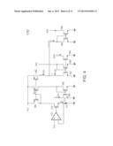
[0030] A synthesis circuit (IAV) 150 is couple to receive the switching current signal VS for generating a synthesis current signal V1. The switching current signal VS is only available during the on time TON of the switching signal SW. Because the transistor 30 is turned off, the switching current signal VS is at a zero value during the off time of the switching signal SW, which is shown in FIG. 1A and FIG. 1B. The synthesis circuit 150 is utilized to emulate the switching current IL during the discharge period of the inductor 20 (the turned-off period of the switching signal SW). Thus, the synthesis current signal VI includes the switching current signal VS and its discharge signal in the discharge period. The signal VFB, the input-voltage signal IAC, and the switching signal SW are coupled to the synthesis circuit 150 for emulating the discharge signal. The synthesis circuit 150 further generates signals IVO and IVIN coupled to a detection circuit (DET) 200. The signal IVO is correlated to the level of the output voltage VO. The signal IVIN is correlated to the level of the input voltage VIN. The detection circuit 200 is coupled to receive the switching signal SW, the input-voltage signal IAC, and a pulse signal PLS for generating a CCM signal SCCM (mode signal). The CCM signal SCCM is used to indicate the CCM or DCM operation. For example, in the embodiment, the CCM signal SCCM is generated (enabled) when the switching current IL is operated in the CCM.
[0031] A transconductance amplifier (Gm) 120 receives the switching-current command signal VM and the synthesis current signal VI for generating a current loop signal IEA. The capacitor 53 is coupled to the current loop signal IEA for the current loop compensation. Current sources 125 and 127 form a bias current IB2 for the transconductance amplifier 120. The current source 127 is turned off during the DCM operation and turned on during the CCM operation. A switch 145 and the current source 127 are coupled between the transconductance amplifier 120 and the ground in series. The switch 145 is controlled to be turned on or off by the CCM signal SCCM through an inverter 140. Accordingly, the on/off state of the current source 127 is controlled by the CCM signal SCCM via the inverter 140 and the switch 145. The bias current IB2 will provide a maximum output current for the transconductance amplifier 120. The maximum output current of the transconductance amplifier 120 associated with the capacitor 53 determines the current loop signal IEA. A pulse width modulation (PWM) circuit (PWM) 300 generates the switching signal SW in accordance with the current loop signal ILA. The PWM circuit 300 further generates the signal PLS coupled to the detection circuit 200.
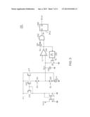
[0032] FIG. 3 is a preferred embodiment of the synthesis circuit 150 according to the present invention. An amplifier 160 cooperating with resistors 161-163 is coupled to sample the switching current signal VS via a switch 165 during the on time of the switching signal SW. The switching current signal VS is hold in a capacitor 167 after the switch 165 is turned off. An emulation circuit 170 generates a discharge current IDS in response to the signals VFB and the input-voltage signal IAC. The discharge current IDS is coupled to discharge the capacitor 167 for emulating the discharge signal of the synthesis current signal VI during the discharge period of the inductor 20. The emulation circuit 170 further generates the signals IVO and IVIN coupled to the detection circuit 200.
[0033] The emulation circuit 170 is developed for generating the discharge current IDS. The detailed operation for the discharge (demagnetizing) of the inductor can be found in a prior art "Method and apparatus for detecting demagnetizing time of magnetic device", U.S. Pat. No. 7,471,523.
T DS = T ON × k × V IN ( V O - V IN ) ( 7 ) ##EQU00002##
[0034] wherein k is a constant.
[0035] The discharge current IDS is correlated to the discharge time TDS. The input-voltage signal IAC is correlated to the input voltage VIN. The signal VFB is correlated to the output voltage VO. The discharge current IDS associated with the capacitance of the capacitor 167 determines the discharge time TDS.
[0036] FIG. 4 is a preferred embodiment of the emulation circuit 170 according to the present invention. An amplifier 171, a resistor 173, and a transistor 172 develop a V-to-I converter for generating a current I172 in accordance with the signal VFB. Transistors 180, 181, 182, 185, and 186 form a first current mirror to generate the signal IVO and a current I182. Transistors 192, 193, and 194 form a second current mirror to generate the signal IVIN and a current I192. Transistors 195 and 196 develop a third current mirror to generate the discharge current IDS in response to the current I182 and the current I192.
V FB = V O × R 42 R 41 + R 42 I 182 = { [ V O × R 42 R 41 + R 42 ] / R 173 } × k 1 I 192 = I AC × k 2 I DS = I 182 - I 192 I AC = V IN R 50 ( shown in FIG . 1 ) ( 8 ) ##EQU00003##
[0037] wherein R41, R42, and R173 are the resistance of the resistors 41, 42, and 173 respectively.
[0038] The discharge current IDS shown in Equation (8) can be expressed as Equation (9)
I DS = { [ V O × R 42 R 41 + R 42 ] / R 173 } × k 1 - ( V IN R 50 × k 2 ) ( 9 ) ##EQU00004##
[0039] wherein k1 and k2 are current mirror ratios.
[0040] The charge slope of the switching current signal VS is equal to the discharge slope of the synthesis current signal VI, which is shown in Equation (10)
( V IN L × T ON ) × R 35 × k 3 = I DS C 167 × T DS ( 10 ) ##EQU00005##
[0041] wherein R35 is the resistance of the resistor 35.
[0042] It can be rewritten as Equations (11) and (12),
( V IN L × R 35 × k 3 ) × T ON = 1 C 167 × { [ V O × R 42 R 173 × ( R 41 + R 42 ) ] × k 1 - ( V IN R 50 × k 2 ) } × T DS ( 11 ) V IN × k A × T ON = ( V O × k B - V IN × k C ) × T DS ( 12 ) ##EQU00006##
[0043] wherein R50 is the resistance of the resistor 50; C167 is the capacitance of the capacitor 167, and
k A = ( 1 L × R 35 × k 3 ) ##EQU00007## k B = 1 C 167 × R 42 R 173 × ( R 41 + R 42 ) × k 1 ##EQU00007.2## k C = 1 R 50 × k 2 ##EQU00007.3## set k B = k C ; ##EQU00007.4## and ##EQU00007.5## k = k A k B ##EQU00007.6##
[0044] Equation (12) can be rewritten as Equation (7).
T DS = T ON × k × V IN ( V O - V IN ) ##EQU00008##
[0045] FIG. 5 is a preferred embodiment of the detection circuit 200 according to the present invention. The signal IVIN is coupled to charge a capacitor 230 via transistors 210, 211, 215, and 216 and a switch 220 during on time of the switching signal SW. When the switching signal SW is turned off, the signal IVO and the signal IVIN are coupled to discharge the capacitor 230 via a switch 225 and a transistor 217 during the discharge time TDS. A discharge signal SD controls the switch 225. The enable of the discharge signal SD indicates the discharge time TDS. The switching signal SW controls the switch 220. According to the rising edge of the switching signal SW, a pulse generator 250 generates a pulse signal Sp coupled to discharge the capacitor 230 through a transistor 251. A saw signal S230 is thus generated in the capacitor 230 in response to the switching signal SW.
[0046] A comparator 240 is utilized to compare the saw signal S230 with a threshold VT. The output of the comparator 240 is coupled to enable the discharge signal SD via an AND gate 242 and an inverter 241 when the switching signal SW is turned off and the saw signal S230 is higher than the threshold VT. The discharge signal SD and the pulse signal PLS are coupled to a flip-flop 260 for generating the CCM signal SCCM. The rising edge of the pulse signal PLS is applied to enable the switching signal SW and latch the status of the discharge signal SD (in the flip-flop 260). If the switching signal SW is enable (starting a switching cycle) before the end of the discharge time TDS (the discharge signal SD), then the switching operation is a CCM. Equation (13) shows the operation of the detection circuit 200.
(IVIN×ka)×TON=(IVO-IVIN×kb)×- TDS (13)
[0047] Equation (13) can be expressed as Equation (14)
(VIN×kc)×TON=(Vo×kd-VIN×ke).times- .TDS (14)
set the kd=ke and
k = kc kd , ##EQU00009##
then Equation (14) will be same as Equation (7). Where ka, kb, kc, kd, and ke are the constant determined by the circuit parameters.
[0048] FIG. 6 shows a reference circuit for the PWM circuit 300. An oscillator (OSC) 310 generates the pulse signal PLS and a ramp signal RMP. The pulse signal PLS is coupled to generate the switching signal SW and provide a dead-time for the switching signal SW. The ramp signal RMP is coupled to compare with the current loop signal IEA for the reset of a flip-flop 350 via a comparator 320. Through an AND gate 360 and an output buffer 365, the flip-flop 350 generates the switching signal SW.
[0049] FIG. 7 shows the waveforms of the ramp signal RMP, the pulse signal PLS, the switching signal SW, and the pulse signal SP.
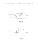
[0050] FIG. 8 is an equivalent circuit of the transconductance amplifier 120. The capacitor 53 is connected to the output of the transconductance amplifier 120. A equivalent output resistance ROT and the capacitance of the capacitor 53 develop a low-pass filter for the current loop signal IEA. The gain Gm of the transconductance amplifier 120 can be expressed,
G m = I OT V INP ##EQU00010##
[0051] wherein IOT is an equivalent current; VINP is differential input voltage of the transconductance amplifier 120.
[0052] FIG. 9 is an equivalent circuit for the circuit shown in FIG. 8.
VOT=IOT×ROT=Gm×VINP×ROT
[0053] However, the maximum output voltage of the transconductance amplifier 120 is limited by its supply voltage VCC, in which the equivalent voltage VOT will be saturated and clamped by the supply voltage VCC in response to a higher value of the differential input voltage VINP. The equivalent output resistance ROT can be expressed as,
R OT = V OT I OT ≈ V OT ( max ) m × I B 2 ≈ V CC m × I B 2 ( 15 ) ##EQU00011##
[0054] where m is a constant.
[0055] In accordance with Equation (15), we can find that the equivalent output resistance (also referring to as output impedance) ROT can be changed by the change of the bias current IB2. The equivalent output resistance ROT associated with the capacitor 53 develops a pole FP for the loop compensation. The pole FP will reduce the current loop gain. A lower bias current IB2 produces a higher equivalent output resistance ROT and a lower frequency pole FP.
F P = I 2 π × R OT × C 53 ##EQU00012##
[0056] According to the present invention, a lower bias current IB2 is utilized to reduce the bandwidth and the current loop gain for stabilizing the CCM operation. A higher bias current IB2 is applied to increase the bandwidth for achieving a better PF value for the PFC power converter.
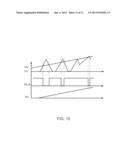
[0057] FIG. 10 shows the waveforms of the switching-current command signal VM, the synthesis current signal VI, the equivalent voltage VOT, and the current loop signal IEA.
[0058] While the invention has been described by way of example and in terms of the preferred embodiments, it is to be understood that the invention is not limited to the disclosed embodiments. To the contrary, it is intended to cover various modifications and similar arrangements (as would be apparent to those skilled in the art). Therefore, the scope of the appended claims should be accorded the broadest interpretation so as to encompass all such modifications and similar arrangements.
User Contributions:
Comment about this patent or add new information about this topic:
| People who visited this patent also read: | |
| Patent application number | Title |
|---|---|
| 20170074213 | APPARATUS AND METHOD FOR OXY-COMBUSTION OF FUELS IN INTERNAL COMBUSTION ENGINES |
| 20170074212 | HYDRAULIC SERVO GAS REGULATOR FOR MULTI-FUEL ENGINE |
| 20170074211 | SYSTEM AND METHOD FOR REDUCING IDLE THRUST IN A TRANSLATING COWL THRUST REVERSER |
| 20170074210 | GAS TURBINE ENGINE WITH AXIAL MOVABLE FAN VARIABLE AREA NOZZLE |
| 20170074209 | GAS TURBINE ENGINE WITH AXIAL MOVABLE FAN VARIABLE AREA NOZZLE |
Images included with this patent application:
 |  |
 |  |
 |  |
 |  |
 |  |
 |  |
 |
| Similar patent applications: | |
| Date | Title |
|---|---|
| 2013-06-20 | Adaptive phase-lead compensation with miller effect |
| 2013-08-01 | Dead-time compensation in a power supply system |
| 2012-03-29 | Adaptive slope-compensation module and method thereof |
| 2013-08-08 | Gradation voltage generating circuit and liquid crystal display device |
| 2012-04-26 | Driver for cooperating with a wall dimmer |
| New patent applications in this class: | |
| Date | Title |
|---|---|
| 2016-12-29 | Pulse width modulation controller architectures |
| 2016-09-01 | Pfc circuit |
| 2016-09-01 | Pfc current shaping |
| 2016-07-14 | Two-stage clocked electronic evergy converter |
| 2016-04-28 | Overall dynamic reactive power control in transmission systems |
| New patent applications from these inventors: | |
| Date | Title |
|---|---|
| 2017-07-13 | Adaptive buck converter and charging cable using the same |
| 2017-07-13 | Mobile device charger for charging mobile device and related adaptive charging voltage generator |
| 2013-08-29 | Digital control circuit for resonant power converters |
| 2013-06-13 | Switching current synthesis circuit for power converter |
| Top Inventors for class "Electricity: power supply or regulation systems" | |
| Rank | Inventor's name |
|---|---|
| 1 | Weihong Qiu |
| 2 | Benjamim Tang |
| 3 | Qian Ouyang |
| 4 | Ta-Yung Yang |
| 5 | John L. Melanson |