Patent application title: PRINTED CIRCUIT BOARD USED IN SERVER
Inventors:
Bo Tian (Shenzhen City, CN)
Bo Tian (Shenzhen City, CN)
Kang Wu (Shenzhen City, CN)
Kang Wu (Shenzhen City, CN)
Assignees:
HON HAI PRECISION INDUSTRY CO., LTD.
HONG FU JIN PRECISION INDUSTRY(ShenZhen) CO., LTD.
IPC8 Class:
USPC Class:
439 55
Class name: Electrical connectors preformed panel circuit arrangement, e.g., pcb, icm, dip, chip, wafer, etc.
Publication date: 2012-10-25
Patent application number: 20120270418
Abstract:
A printed circuit board used in server, which has a golden finger
interface at one side thereof. The golden finger interface includes a
plurality of parallelly arranged metal sheets which conform to the USB
standard. The golden finger interface is used to be engaged with a USB
socket for transmitting the electrical signal.Claims:
1. A printed circuit board (PCB), comprising: a golden finger interface
at one side thereof, the golden finger interface comprising a plurality
of parallel arranged metal sheets, and the golden finger interface being
used to be engaged with a universal serial bus (USB) socket for
transmitting electrical signals; and two spaced slots adjacent to the one
side, the two slots both perpendicular to the one side, the distance
between the two slots being equal to a width of the USB socket, the
golden finger interface being positioned between the two slots, and a
middle portion of the PCB between the two slots being thinner than other
areas of the PCB.
2. The printed circuit board of claim 1, wherein a plurality of grounding holes are defined in the middle portion of the PCB at both sides of the golden finger interface.
3. (canceled)
4. The printed circuit board of claim 1, being a four-layer board, a six-layer board or a ten-layer board.
Description:
BACKGROUNDING
[0001] 1. Technical Field
[0002] The disclosure generally relates to printed circuit boards (PCB), and particularly to a PCB used in a server.
[0003] 2. Description of Related Art
[0004] Universal serial bus (USB) is a specification to establish communication between devices and a host controller (such as a server or a personal computer). However, a USB connector is rarely used when the server is working, so a conventional USB connector would increase the cost.
[0005] It is desirable to provide a PCB used in server having innovative USB means that can reduce the cost.
BRIEF DESCRIPTION OF THE DRAWINGS
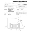
[0006] FIG. 1 is a partial, schematic diagram of a first exemplary embodiment of a PCB.
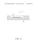
[0007] FIG. 2 is a cross section of the PCB of FIG. 1, taken along line II-II thereof.
DETAILED DESCRIPTION
[0008] Referring to FIGS. 1 and 2, a PCB 1 used in a server according to an exemplary embodiment of the disclosure is shown. The PCB 1 can be a four-layer board, six-layer board or ten-layer board.
[0009] Two spaced slots 10 are defined at one side of the PCB 1. The two slots 10 are both perpendicular to the side of the PCB 1. The distance between the two slots 10 is equal to a traditional USB socket (not shown). In this embodiment, each of the slots 10 is rectangle. The middle of the two slots 10 of the PCB 1 is a four-layer board, and the thickness thereof is thinner than a other area of the PCB 1, so it can be used to be engaged with the traditional USB socket.
[0010] A golden finger interface 20 is positioned between the two slots 10 on the PCB 1. The golden finger interface 20 includes a plurality of parallelly arranged metal sheets 21 which conform to the USB standard, and a length of the metal sheet 21 is shorter than that of the slot 10. The golden finger interface 20 is used to be engaged with the traditional USB socket (not shown) for transmitting the electrical signal.
[0011] A plurality of grounding holes 30 are defined at both sides of the golden finger interface 20 in the PCB 1. When the traditional USB socket is engaged with the golden finger interface 20, the electromagnetic interference is reduced thereof. In this embodiment, the grounding holes 30 are circular shaped, certainly, the grounding holes 30 can be other shaped.
[0012] Understandably, when the PCB 1 as a whole is a four-layer board, the thickness in the middle of the two slots 10 of the PCB 1 is equal to the other area thereof. It is necessary that the thickness in the middle of the two slots 10 thereof matches with the height of the traditional USB socket. The number of the grounding holes 30 can be changed according to need. And the locations of the grounding holes 30 can also be changed to the other places.
[0013] Because the golden finger interface 20 is positioned on the PCB 1 instead of traditional USB connector, the PCB 1 is made simple, used easily at a lower cost.
[0014] It is to be understood, however, that even though numerous characteristics and advantages of certain embodiment(s) have been set forth in the foregoing description, together with details of the structures and functions of the embodiments, the disclosure is illustrative only, and changes may be made in detail, especially in matters of shape, size, and arrangement of parts within the principles of the disclosure to the full extent indicated by the broad general meaning of the terms in which the appended claims are expressed.
User Contributions:
Comment about this patent or add new information about this topic:
Images included with this patent application:
 |  |
 |  |
| Similar patent applications: | |
| Date | Title |
|---|---|
| 2009-10-08 | Printed circuit board |
| 2012-11-15 | Circuit board and method of manufacturing inkjet head |
| 2009-10-01 | Integrated circuit socket set |
| 2009-10-29 | Pothead for use in highly severe conditions |
| 2010-08-05 | Printed circuit assembly |
| New patent applications in this class: | |
| Date | Title |
|---|---|
| 2019-05-16 | Socket connector for an electronic package |
| 2016-02-18 | Discrete packaging adapter for connector |
| 2015-12-17 | Stacked electrical system for connecting a printed circuit board to a busbar |
| 2015-12-10 | Method and apparatus for reducing far-end crosstalk in electrical connectors |
| 2015-11-12 | Flip-cover receptor connector, and rf plate cable and cable end connector used in conjunction therewith |
| New patent applications from these inventors: | |
| Date | Title |
|---|---|
| 2014-03-27 | Heat sink |
| 2014-02-13 | Control circuit for fan |
| 2014-01-02 | Power supply circuit for hard disk drive |
| 2013-12-12 | Test circuit for power supply unit |
| Top Inventors for class "Electrical connectors" | |
| Rank | Inventor's name |
|---|---|
| 1 | Jerry Wu |
| 2 | Noah Montena |
| 3 | Qi-Sheng Zheng |
| 4 | Jun Chen |
| 5 | Norman R. Byrne |