Patent application title: THERMOELECTRIC MATERIAL WITH LOW ELECTRICAL RESISTIVITY AND MANUFACTURE THEREOF
Inventors:
Sinn-Wen Chen (Hsinchu, TW)
Sin-Jie Wu (Hsinchu, TW)
Assignees:
NATIONAL TSING HUA UNIVERSITY
IPC8 Class: AH01B102FI
USPC Class:
252514
Class name: Electrically conductive or emissive compositions free metal containing noble metal (gold, silver, ruthenium, rhodium, palladium, osmium, iridium, platinum)
Publication date: 2012-05-17
Patent application number: 20120119164
Abstract:
Thermoelectric material has attracted more attentions as a promising
energy material in recent years. Research nowadays are devoted to
improvement of figure-of-merit (zT=S2T/ρκ). Motivated by
p-type AgSbTe2 compound, ternary Ag--Sb--Te has been reported as an
important thermoelectric system. Although ternary AgSbTe2 compound
has been considered as a candidate for thermoelectric materials with the
advantages of low thermal conductivity (κp=0.6 WK-1
m-1), the relatively high electrical resistivity
(ρ=7.5*10-3 Ωcm) has limited its applications. This
invention disclosed brand-new Ag--Sb--Te bulk materials with very fine
microstructures that nanoscale Ag2Te phase precipitate uniformly in
the multi-phase matrix through class I reaction,
liquid=Ag2Te+AgSbTe2+δ. Moreover, the electrical
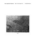
resistivity (ρ) measured by four-probe method is as low as
8.4*10-4 (Ωcm) at room temperature, which guarantees the
promise of those ternary bulk materials.Claims:
1. A thermoelectric material with low electrical resistivity, comprising
Ag, Sb and Te in a molar ratio of 1:2.43.about.3.29:2.18.about.2.96,
wherein the electrical resistivity of the thermoelectric material is less
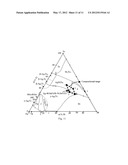
than 0.1 Ωcm at room temperature.
2. The thermoelectric material as claimed in claim 1, wherein Ag, Sb and Te are constituted in a molar ratio of 1:2.55.about.3.15:2.31.about.2.83
3. The thermoelectric material as claimed in claim 1, wherein the average crystal grain size of the thermoelectric material is preferably less than 1000 nm.
4. The thermoelectric material as claimed in claim 1, wherein the average crystal grain size of the thermoelectric material is preferably less than 500 nm.
5. The thermoelectric material as claimed in claim 1, wherein Ag, Sb and Te are constituted in a total weight ratio of 90% or more.
6. The thermoelectric material as claimed in claim 1, wherein the electrical resistivity of the thermoelectric material is preferably less than 0.01 Ωcm at room temperature.
7. A thermoelectric material with low electrical resistivity made by the steps of: (A) providing a initial material comprising Ag, Sb and Te in a molar ratio of 1:2.43.about.3.29:2.18.about.2.96; (B) melting the initial material in vacuum with a temperature of at least 500.degree. C. for a predetermined period; and (C) quenching the initial material for a predetermined period to form the thermoelectric material; wherein the thermoelectric material is less than 0.1 Ωcm at room temperature.
8. The manufacture as claimed in claim 7, wherein the initial material in step (B) is melted for 24 hours.
9. The manufacture as claimed in claim 7, wherein the initial material in step (C) is firstly quenched to 550.degree. C. with a rate of 1.degree. C./min, secondly quenched at this temperature for 120 hours, and finally quenched again by cool water.
10. The manufacture as claimed in claim 7, wherein the initial material in step (C) is rapidly quenched in first, secondly quenched at 650.degree. C. in a furnace for 120 hours, and finally quenched by cool water.
Description:
CROSS-REFERENCED TO RELATED APPLICATIONS
[0001] This Non-provisional application claims priority under 35 U.S.C. §119(a) on Patent Application No. 099139575 filed on Nov. 17, 2010 Republic of China, the entire contents of which are hereby incorporated by reference.
FIELD OF THE INVENTION
[0002] The present invention relates a thermoelectric material with low electrical resistivity in comparison with a conventional metal or semiconductor.
BACKGROUND OF THE INVENTION
[0003] The thermoelectric material is a solid material which can convert thermal energy into electrical energy or use electrical energy to move heat. In 1821, Thomas Johann Seebeck found that a circuit made from two dissimilar metals (Cu and Bi), with junctions at different temperatures (ΔT) would generate an electric potential (ΔV), which is defined as Seebeck coefficient (S=ΔV/ΔT), and used as a principle for the thermoelectric generator and thermocouple. In 1835, Jean Charles Athanase Peltier found that an electrical current would produce heating or cooling at the junction of two dissimilar metals, and this principle was used for thermoelectric cooler. Twenty years later, William Thomson established the base of thermoelectric theory and predicted a third thermoelectric effect, now known as the Thomson effect. In the Thomson effect, heat is absorbed or produced when current flows in a material with a temperature gradient. The heat is proportional to both the electric current and the temperature gradient.
[0004] The thermoelectric material has been developed more than one hundred years so far. How to obtain better thermoelectric conversion efficiency was the most important goal for its applicability. Until 1954, Goldsmid and Douglas etc. applied semiconductor materials to thermoelectric coolers and successfully lowered down cooling temperature to 0° C., this huge progress induced a studying heat in 1960. However, for the past 30 years, this field has fallen in a difficult position. Until 1990, various novel materials have been developed so as to inspire studies in this field. Thermoelectric materials often involve the multi-component system, and complex composition and synthesis condition limit its utility. At present, it is a major object to develop novel thermoelectric materials and thermoelectric components.
[0005] In thermoelectric material developments, thermoelectric figure of merit (z=S2/κρ; S: Seebeck coefficient; κ=thermal conductivity, ρ=electrical resistivity) is an important indicator for developments. Nowadays the most popular commercial thermoelectric material is p-type semiconductor Bi2Te3, whose thermoelectric figure of merit is 1. Hsu etc. (Science, Vol. 303, pp. 818-821, 2004) has published a paper about high-performance thermoelectric material AgPbmSbTe2+m, which indicated that nano structure could help its thermoelectric conversion efficiency and its thermoelectric figure of merit reached 2.2 at 800 K. Therefore, how to obtain better thermoelectric conversion efficiency has become a crucial object.
SUMMARY OF THE INVENTION
[0006] Ag--Sb--Te is a material system deserved to study. AgSbTe2 is an existed ternary compound and also a p-type semiconductor having low thermal conductivity and high thermoelectric conversion efficiency (thermoelectric figure of merit is approximately 1.4). However, its high resistivity and fragile characteristic significantly influence its applicability.
[0007] It is an object of the present invention to provide a thermoelectric material Ag--Sb--Te having low resistivity.
[0008] In one aspect of the present invention, thermoelectric material with low electrical resistivity comprising: at least Ag, Sb and Te, in a molar ratio of 1:2.43˜3.29:2.18˜2.96, wherein the electrical resistivity of the thermoelectric material is less than 0.1 Ωcm at room temperature.
[0009] Preferably, Ag, Sb and Te are constituted in a molar ratio of 1:2.55˜3.15:2.31˜2.83.
[0010] Preferably, the average crystal grain size of the thermoelectric material is preferably less than 1000 nm.
[0011] Preferably, the average crystal grain size of the thermoelectric material is preferably less than 500 nm.
[0012] Preferably, Ag, Sb and Te are constituted in a total weight ratio of 90% or more.
[0013] Preferably, the electrical resistivity of the thermoelectric material is preferably less than 0.01 Ωcm at room temperature.
[0014] In another aspect of the present invention, manufacture of preparing a thermoelectric material with low electrical resistivity, comprising the steps of: (A) providing a initial material comprising Ag, Sb and Te in a molar ratio of 1:2.43˜3.29:2.18˜2.96; (B) melting the initial material in vacuum with a temperature of at least 500° C. for a predetermined period; and (C) quenching the initial material for a predetermined period to form the thermoelectric material; wherein the thermoelectric material is less than 0.1 Ωcm at room temperature.
[0015] Preferably, the initial material in step (B) is melted for 24 hours.
[0016] Preferably, the initial material in step (C) is firstly quenched to 550° C. with a rate of 1° C./min, secondly quenched at this temperature for 120 hours, and finally quenched again by cool water.
[0017] Preferably, the initial material in step (C) is rapidly quenched in first, secondly quenched at 650° C. in a furnace for 120 hours, and finally quenched by cool water.
[0018] Resistivity of the thermoelectric material of the present invention is 8.4*10-4 Ωcm measured by four point probe method at room temperature, and it is one-tenth of that in ternary compound AgSbTe2. According to following analysis and material, the phase formation is proved to be AgSbTe2, δ phase (Sb2Te) and 200-400 nm Ag2Te phase. These results prove that it is an ideal thermoelectric material which is suitable to be applied to modules of thermoelectric generators, industry thermal recycling, and combination with other energy materials such as solar cells. As expected, in the future, new energy materials developed by the thermoelectric material with low resistivity of the present invention may play a crucial role in new energy technology developments.
[0019] The embodiments of the present invention are further described through below detailed examples and the drawings.
BRIEF DESCRIPTION OF THE DRAWINGS
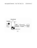
[0020] FIG. 1 is a schematic diagram showing the manufacture of the present invention.
[0021] FIG. 2 is a metallographic diagram showing the material of Ag-40.0 at % Sb-36.0 at % Te at low magnification.
[0022] FIG. 3 is a metallographic diagram showing the material of Ag-40.0 at % Sb-36.0 at % Te at high magnification.
[0023] FIG. 4 is a diagram showing electrical resistivities of the material of the present invention in comparison with other high efficiency thermoelectric materials.
[0024] FIG. 5 is a metallographic diagram showing the material of Ag-40.0 at % Sb-36.0 at % Te at low magnification.
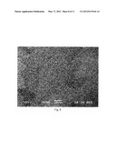
[0025] FIG. 6 is a metallographic diagram showing the material of Ag-40.0 at % Sb-36.0 at % Te at high magnification.
[0026] FIG. 7 is a diagram showing electrical resistivities of the material of the present invention in comparison with other high efficiency thermoelectric materials.
[0027] FIG. 8 is a metallographic diagram showing the material of Ag-40.0 at % Sb-36.0 at % Te at low magnification.
[0028] FIG. 9 is a metallographic diagram showing the material of Ag-40.0 at % Sb-36.0 at % Te at high magnification.
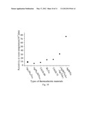
[0029] FIG. 10 is a diagram showing electrical resistivities of the material of the present invention in comparison with other high efficiency thermoelectric materials.
DETAILED DESCRIPTION
[0030] A thermoelectric material with low electrical resistivity and manufacture thereof are described with reference to the preferred embodiments below, it is apparent to those skilled in the art that a variety of modifications and changes may be made without departing from the scope of the present invention which is intended to be defined by the appended claims.
DEFINITION
[0031] The formula "Ag-40.0 at % Sb-36.0 at % Te" wherein at % represents the atomic percent of each element in that alloy.
[0032] The compositional range of Ag-40.0 at % Sb-36.0 at % Te is determined by the liquidus projection constructed by experiments. During the cooling process, melts with nominal compositions located in that compositional range (Ag, Sb and Te in a molar ration of 1:2.43˜3.29:2.18˜2.96) will pass through the ternary eutectic point (Ag-40.0 at % Sb-36.0 at % Te), and solidify large amount of nano-sized phase.
[0033] The compositional range is indicated by a square. Alloys within that square area will exhibit large amount of the eutectic phase (Ag-40.0 at % Sb-36.0 at % Te) in their solidification microstructures. (as show in FIG. 11) The compositions of points 1, 2, 3 and 4 are: (1) Ag-38.0 at % Sb-47.0 at % Te (Ag:Sb:Te=1:2.43:2.96 in molar ration), (2) Ag-43.3 at % Sb-38.8 at % Te (Ag:Sb:Te=1:2.43:2.18 in molar ration), (3) Ag-45.3 at % Sb-40.8 at % Te (Ag:Sb:Te=1:3.29:2.96 in molar ration), (4) Ag-50.8 at % Sb-33.7 at % Te (Ag:Sb:Te=1:3.29:2.18 in molar ration). The specific compositional range as stated in the claim 1 (Ag, Sb and Te in a molar ratio of 1:2.43˜3.29:2.18˜2.96) is determined thereby.
Embodiment 1
[0034] (i) Metallographic and Composition Analysis
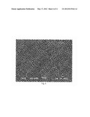
[0035] With reference to FIG. 1, it demonstrates the manufacture of the present invention. A predetermined amount of silver (Ag), antimony (Sb), and Tellurium (Te) in high purity was weighted by the electronic scale (Mettler, Ae200, USA) to prepare an alloy in a ratio of Ag-40.0 at % Sb-36.0 at % Te, and the prepared alloy was placed in a 6 mm×8 mm quartz tube. In order to prevent oxidation of the alloy, it was sealed by an oxygen-gas torch gun in a vacuum of 2×10⁻⁵ bar. The alloy was placed in a furnace at 800° C. to melt for 24 hours, and then quenched by cool water to prevent generation of low-temperature solid phase. Then the alloy was cold mount by resin to perform metallographic and composition analysis. The alloy was ground by the sandpapers of #1200, #2400, and #4000, and was polished by aluminum oxide powder of 1.0 μm and 0.3 μm to. Until a mirror surface was shown, residual powder was removed by a sonicator. An optical microscope (OM, Olympus, BH, Japan) was used for initial observation, and then an scanning electronic microscope (SEM, Hitachi, S-2500, Japan) and an electron probe microanalyzer (Electron Probe Microanalysis, EPMA; JEOL, JXA-8600 SX, Japan) were used for the composition analysis. The results were shown in FIGS. 2 and 3, which were metallographic diagrams showing the material of Ag-40.0 at % Sb-36.0 at % Te at different magnification. In FIG. 2, there was no distinguished phase. In FIG. 3, the dotted phase in a grain size of 200-400 nm was uniformly distributed in the alloy, and this nano-size microstructure was a characteristic of the present invention.
[0036] (ii) Electrical Property Measurement
[0037] The composition and manufacture of the alloy were described as (i), the quenched alloy cylinder was cut by a diamond sawing blade (BUEHLER® IsoMet®, U.S.A) to form a round ingot of 1 mm thickness and 6 mm diameter, and resistivity (Ωcm) of the ingot was then measured by Van der Pauw and four point probe method at room temperature. The 20W Model 2400 SourceMeter® instrument was used, 1 A of input was selected and resistance (Ω) was measured and displayed. By proper calibration and calculation, measured resistivity (ρ) was 7.72*10-4 (Ωcm). FIG. 4 was a diagram showing electrical resistivity of the material of the present invention in comparison with other high efficiency thermoelectric materials. As compared in FIG. 4, the thermoelectric material of the present invention had an extremely low resistivity.
Embodiment 2
[0038] (i) Metallographic and Composition Analysis
[0039] In this embodiment, most of the steps are similar with embodiment 1. At first, a predetermined amount of silver (Ag), antimony (Sb), and Tellurium (Te) in high purity was weighted by the electronic scale (Mettler, Ae200, USA) to prepare an alloy in a ratio of Ag-40.0 at % Sb-36.0 at % Te, and the prepared alloy was placed in a 6 mm×8 mm quartz tube. In order to prevent oxidation of the alloy, it was sealed by an oxygen-gas torch gun in a vacuum of 2×10⁻⁵ bar. The alloy was placed in a furnace at 800° C. to melt for 24 hours, and the alloy was firstly quenched to 550° C. with a rate of 1° C./min, secondly quenched at this temperature for 120 hours, and finally quenched again by cool water. Then the alloy was cold mount by resin to perform metallographic and composition analysis. The following steps were the same as described in embodiment 1 and not repeated herein. The results were shown in FIGS. 5 and 6, which were metallographic diagrams showing the material of Ag-40.0 at % Sb-36.0 at % Te at different magnification. In FIG. 5, there was no distinguished phase. In FIG. 6, the dotted phase in a grain size of 200-400 nm was uniformly distributed in the alloy, and this nano-size microstructure was a characteristic of the present invention.
[0040] (ii) Electrical Property Measurement
[0041] The composition and manufacture of the alloy were described as (i), the quenched alloy cylinder was cut by a diamond sawing blade (BUEHLER® IsoMet®, U.S.A) to form a round ingot of 1 mm thickness and 6 mm diameter, and resistivity (Ωcm) of the ingot was then measured by Van der Pauw and four point probe method at room temperature. The 20W Model 2400 SourceMeter® instrument was used, 1 A of input was selected and resistance (Ω) was measured and displayed. By proper calibration and calculation, measured resistivity (ρ) was 8.33*10-4 (Ωcm). FIG. 7 was a diagram showing electrical resistivity of the material of the present invention in comparison with other high efficiency thermoelectric materials. As compared in FIG. 7, the thermoelectric material of the present invention had an extremely low resistivity.
Embodiment 3
[0042] (i) Metallographic and Composition Analysis
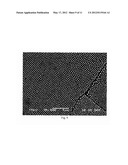
[0043] In this embodiment, most of the steps are similar with embodiment 1. At first, a predetermined amount of silver (Ag), antimony (Sb), and Tellurium (Te) in high purity was weighted by the electronic scale (Mettler, Ae200, USA) to prepare an alloy in a ratio of Ag-40.0 at % Sb-36.0 at % Te, and the prepared alloy was placed in a 6 mm×8 mm quartz tube. In order to prevent oxidation of the alloy, it was sealed by an oxygen-gas torch gun in a vacuum of 2×10⁻⁵ bar. The alloy was placed in a furnace at 800° C. to melt for 24 hours. After rapid cooling, the alloy was quenched at 650° C. for 120 hours, and then quenched again by cool water. Then the alloy was cold mount by resin to perform metallographic and composition analysis. The following steps were the same as described in embodiment 1 and not repeated herein. The results were shown in FIGS. 8 and 9, which were metallographic diagrams showing the material of Ag-40.0 at % Sb-36.0 at % Te at different magnification. In FIG. 8, there was no distinguished phase. In FIG. 9, the dotted phase in a grain size of 200-400 nm was uniformly distributed in the alloy, and this nano-size microstructure was a characteristic of the present invention.
[0044] (ii) Electrical Property Measurement The composition and manufacture of the alloy were described as (i), the quenched alloy cylinder was cut by a diamond sawing blade (BUEHLER® IsoMet®, U.S.A) to form a round ingot of 1 mm thickness and 6 mm diameter, and resistivity (Ωcm) of the ingot was then measured by Van der Pauw and four point probe method at room temperature. The 20W Model 2400 SourceMeter® instrument was used, 1 A of input was selected and resistance (Ω) was measured and displayed. By proper calibration and calculation, measured resistivity (ρ) was 9.33*10-4 (Ωcm). FIG. 10 was a diagram showing electrical resistivity of the material of the present invention in comparison with other high efficiency thermoelectric materials. As compared in FIG. 10, the thermoelectric material of the present invention had an extremely low resistivity.
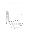
[0045] As depicted in the above embodiments, the thermoelectric material of the present invention had a uniformly nano-size microstructure, and its average resistivity was about 8.46*10-4 Ωcm. Other high efficiency thermoelectric materials in the previous documents were listed in table. 1. According to table. 1, resistivity of the thermoelectric material of the present invention was lower than those in other thermoelectric materials, such as Bi2Te3, AgSbTe2, (AgSbTe2)0.8, (Ag2Te)0.2(Ag2Te)0.2 and TAGS-75, which proved it was a ideal thermoelectric material.
TABLE-US-00001 TABLE 1 Average resistivity of the thermomaterial of the present invention in comparison with those in other materials in previous documents. ρ(Ωcm) at room temperature Reference Ag - 40.0 wt % 8.4 × 10⁻⁴ the persent invention Sb - 36.0 wt % Te Bi2Te3 1.5 × 10⁻³ Ji et al., J. Appl. Phys., 104, 034907, (2008). AgSbTe2 7.5 × 10⁻³ V. Jovovic and J. P. Heremans PHYSICAL REVIEW B, 77, 245204, (2008). AgPbmSbTe2m 5.7 × 10⁻⁴ K. F. Hsu et al., Science, 6, 818, 303, (2004). (AgSbTe2)0.8(Ag2Te)0.2 3.0 × 10⁻³ T. Su et al., Materials Letters, 62, 3269, (2008). TAGS-75 1.6 × 10⁻³ S. H. Yang et al., Nanotechnology, TAGS-80 8.0 × 10⁻⁴ 19, 245707, (2008).
[0046] New energy material belongs to one of the top five development fields. To correspond flourish developments in energy industry, the present invention provides a thermoelectric material which has low resistivity and uniform nano size microstructure, and it can be produced by a simple manufacture. The present invention clearly discloses the embodiments of thermoelectric material, which can be applied to modules of thermoelectric generators, industry thermal recycling, and combination with other energy materials such as solar cells. Therefore, the present invention meets the requirement of utility. The thermoelectric material and its manufacture of the present invention can be used as a critical material required in developments of new energy materials. Further, there was no application about Ag--Sb--Te thermoelectric material with low resistivity and uniform nano size microstructure in the past. Therefore, the present invention also meets the requirements of novelty and unobvious.
[0047] According to the report of BBC Research & Consulting company, the market of new energy equipment and materials in 2009 is estimated as 116 hundred million dollars, and it is expected to increase to 116 hundred million dollars until 2014. Compound Annual Growth Rate (CAGR) has reached 7.8% in the resent five years, and the photothermal material possesses the highest ratio. Its market cost 83 hundred million dollars in 2009, and its CAGR reached 9.8%. Therefore, the invention can meet the requirement of this growing market.
[0048] Although the present invention is described with reference to the preferred embodiments thereof, it is apparent to those skilled in the art that a variety of modifications and changes may be made without departing from the scope of the present invention which is intended to be defined by the appended claims.
User Contributions:
Comment about this patent or add new information about this topic:
| People who visited this patent also read: | |
| Patent application number | Title |
|---|---|
| 20120267077 | COOLING APPARATUSES AND POWER ELECTRONICS MODULES COMPRISING THE SAME |
| 20120267076 | SYSTEM FOR RECOVERING WASTE HEAT |
| 20120267075 | COOLING SYSTEM FOR RECIPROCATING COMPRESSORS AND A RECIPROCATING COMPRESSOR |
| 20120267074 | COOLING DEVICE |
| 20120267073 | COOLING APPARATUS |
Images included with this patent application:
 |  |
 |  |
 |  |
 |  |
 |
| New patent applications in this class: | |
| Date | Title |
|---|---|
| 2018-01-25 | Electroconductive silver paste |
| 2016-06-30 | Nanostructure dispersions and transparent conductors |
| 2016-06-30 | Conductive ink |
| 2016-06-02 | Nanostructure having metal nanoparticles and a method of assembly thereof |
| 2016-06-02 | Method for preparing nano-silver powder and application in preparation of electrically conductive ink of the nano-silver powder and electrically conductive ink |
| New patent applications from these inventors: | |
| Date | Title |
|---|---|
| 2009-07-23 | Metallic dental devices with tooth colors and their preparation methods |
| Top Inventors for class "Compositions" | |
| Rank | Inventor's name |
|---|---|
| 1 | Masayuki Saito |
| 2 | Mingjie Zhou |
| 3 | Steven Tierney |
| 4 | Volker Reiffenrath |
| 5 | Norikatsu Hattori |