Patent application title: LED BACKLIGHT MODULE
Inventors:
Yung-Lun Huang (Taipei, TW)
Assignees:
HON HAI PRECISION INDUSTRY CO., LTD.
IPC8 Class: AF21V722FI
USPC Class:
362606
Class name: Illumination edge lighted panel light modifier with emission face combined with light guide plate
Publication date: 2011-12-01
Patent application number: 20110292678
Abstract:
An LED backlight module includes at least one LED and a light guide
plate. The light guide plate includes a light incident surface, a light
emitting surface connected to the light incident surface, and a bottom
surface parallel to the light emitting surface. The at least one LED is
placed on the light incident surface and spaced at regular intervals. The
light from the at least one LED enters the light guide plate from the
light incident surface and is reflected to the light emitting surface by
the bottom surface. The light guide plate defines a plurality of concave
dots on the bottom surface. The bottom surface is divided into a
plurality of discontinuous dot zones. In the dot zone closest to the
incident surface, proximity of the dot to the LED decreases the depth and
the distribution density of the dots.Claims:
1. An LED backlight module comprising at least one LED and a light guide
plate including a light incident surface, a light emitting surface
connected to the light incident surface, and a bottom surface parallel to
the light emitting surface, wherein the at least one LED is placed on the
light incident surface and spaced at regular intervals, the light from
the at least one LED gets into the light guide plate from the light
incident surface and is reflected to the light emitting surface by the
bottom surface, the light guide plate defines a plurality of concave dots
on the bottom surface, the bottom surface is divided into a plurality of
discontinuous dot zones, in the dot zone closest to the light incident
surface, the closer of the dots to the at least one LED, the lesser of
the depth and the distribute density of the dots are.
2. The LED backlight module of claim 1, wherein the dots in other dot zones beside the dot zone closet to the light incident surface are arranged in array and the dots in the same dot zone are with the same intensity and depth, and the dots in one of the other dot zones farther from the light incident surface are larger in density than those in another of the other dot zones closer to the light incident surface.
3. The LED backlight module of claim 2, wherein the dots in the other dot zones beside from the light incident surface.
4. The LED backlight module of claim 3, wherein the number of the dot zones is four and the depths of the dots from the second closest dot zone to the most far dot zone are 2.5 μm, 3.3 μm, and 3.5 μm.
5. The LED backlight module of claim 4, wherein the depth of the dots in the dot zone closest to the light incident surface are proportional to the distance from the at least one LED in a range from 2 μm to 2.5 μm.
6. The LED backlight module of claim 2, wherein a light mixing area is defined between every two dot zones and the depth of the dots in the light mixing area becomes gradually larger away from the light incident surface.
Description:
BACKGROUND
[0001] 1. Technical Field
[0002] The present disclosure generally relates to LED technology, and particularly to an LED backlight module.
[0003] 2. Description of the Related Art
[0004] Light emitting diodes (LEDs) have many advantages, such as high luminosity, low operational voltage, low power consumption, compatibility with integrated circuits, easy driving, long-term reliability, and environmental friendliness. All of these reasons have promoted the LEDs as a widely used light source. Light emitting diodes are commonly applied in lighting applications.
[0005] LED backlight modules must overcome illumination uniformity challenges. An LED backlight module is commonly arranged with a light guide plate and a plurality of LEDs at the periphery of the light guide plate. The illumination of LED in the light guide plate is not uniform. This will affect the performance of the LED backlight module.
[0006] What is needed, therefore, is an LED backlight module, which can improve illumination uniformity, and ameliorate the described limitations.
BRIEF DESCRIPTION OF THE DRAWINGS
[0007] Many aspects of the disclosure can be better understood with reference to the drawings. The components in the drawings are not necessarily drawn to scale, the emphasis instead being placed upon clearly illustrating the principles of the LED backlight module. Moreover, in the drawings, like reference numerals designate corresponding parts throughout the views.
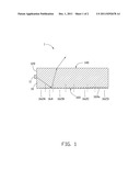
[0008] FIG. 1 is a schematic view of an LED backlight module in accordance with a first embodiment.
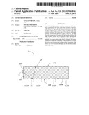
[0009] FIG. 2 is a schematic view of dot pattern distribution on the bottom surface of a light guide plate of FIG. 1.
DETAILED DESCRIPTION
[0010] Embodiments of an LED backlight module as disclosed are described in detail here with reference to the drawings.
[0011] Referring to FIG. 1 and FIG. 2, an LED backlight module 1 in accordance with a first embodiment includes a light guide plate 10 and at least one LED 11 arranged at one side of the periphery of the light guide plate 10. The light guide plate 10 includes a light incident surface 120, a light emitting surface 140, and a bottom surface 160.
[0012] In this embodiment, the light incident surface 120 is connected to the light emitting surface 140, and the bottom surface 160 is parallel to the light emitting surface 140 and connected with the light incident surface 120. The at least one LED 11 is arranged on the light incident surface 120 to allow light from the at least one LED 11 into the light guide plate 10 through the light incident surface 120 and then be reflected by the bottom surface 160 to be emitted through the light emitting surface 140.
[0013] The light guide plate 10 is a rectangular slab and can also be high transparent material, such as resin, epoxy, silicone, polycarbonate (PC), noryl, polybutylene terephthalate (PBT), polyphthalamide (PPA), polypropylene (PP), polymethyl methacrylate (PMMA), glass fiber, TiO2, CaCO3, or a combination thereof. The at least one LED 11 can be arranged in array and spaced at regular intervals on the light incident surface 120.
[0014] The bottom surface 160 defines a plurality of concave dots 160a, each comprising a circular depression. The depth of the concave dot 160a is the vertical distance from the farthest point of the concave dot 160a to the bottom surface 160. In this embodiment, the bottom surface 160 sequentially defines four discontinuous dot zones 162A, 162B, 162C, and 162D away from the light incident surface 120.
[0015] Other than 162A, the closest dot zone to the light incident surface 120, the concave dots 160a in 162B, 162C, and 162D are arranged in array, and the depth and the distribution density of concave dots 160a in the same dot zone perpendicular to the light incident surface 120 are the same. The depths and the distribution densities of concave dots 160a in different dot zones 162B, 162C, and 162D are different. The depth and the distribution density of concave dots 160a in one of the dot zones 162B, 162C, and 162D near the light incident surface 120 exceed those in another of the dot zones 162B, 162C, and 162D farther from the light incident surface 120.
[0016] A light mixing area 164 is defined between every two dot zones 162, such as 162A and 162B, 162B and 162C, 162C and 162D. The depth of the concave dots 160a becomes gradually larger away from light incident surface 10 in the light mixing area 164.
[0017] In the dot zone 162A, the closest dot zone to the light incident surface 120, the depth and distribution density of the concave dots 160a more near the at least one LED 11 is smaller, and the depth and distribution density of the concave dots 160a more far from the at least one LED 11 is larger.
[0018] For example, as shown in FIG. 2, the length L of the bottom surface 160 is 220 mm, and the width W of the bottom surface 160 is 130 mm. The bottom surface 160 defines sequentially four dot zones 162A, 162B, 162C, and 162D with length of 130 mm away from the light incident surface 120. The width W1 of the dot zone 162A is 30 mm, and the width W2 of the dot zones 162B, 162C, and 162D is 45 mm. The depth of the concave dot 160a in the dot zone 162B is 2.5 μm. The depth of the concave dot 160a in the dot zone 162C is 3.3 μm. The depth of the concave dot 160a in the dot zone 162D is 3.5 μm. The dot zone 162A is the closest to the light incident surface 120, the depth and distribution density of the concave dots 160a are proportional to the distance from the at least one LED 11 in a range from 2 μm to 2.5 μm.
[0019] With depth of the concave dot 160a increased more light is reflected to be emitted from the light emitting surface 140. The design of depth of the concave dot 160a proportional to the distance from the at least one LED 11 will eliminate the hot spot on the light emitting surface 140 on the side near the light source and the dark lane on the light emitting surface 140 on the side away from the light source.
[0020] The design of depth of the concave dot 160a in the light mixing area 164 increasing gradually from the dot zone of smaller depth to the dot zone of larger depth will mix thoroughly light reflected from different dot zones and increase enormously the illumination uniformity of the light guide plate 10.
[0021] It is to be understood, however, that even though numerous characteristics and advantages of the disclosure have been set forth in the foregoing description, together with details of the structures and functions of the embodiment(s), the disclosure is illustrative only, and changes may be made in detail, especially in matters of shape, size, and arrangement of parts within the principles of the disclosure to the full extent indicated by the broad general meaning of the terms in which the appended claims are expressed.
User Contributions:
Comment about this patent or add new information about this topic:
Images included with this patent application:
 |  |
 |
| Similar patent applications: | |
| Date | Title |
|---|---|
| 2008-10-30 | Optical plate and backlight module using the same |
| 2008-10-30 | Optical plate and backlight module using the same |
| 2008-10-30 | Optical plate and backlight module using the same |
| 2008-10-30 | Optical plate and backlight module using the same |
| 2008-10-30 | Optical plate and backlight module using the same |
| New patent applications in this class: | |
| Date | Title |
|---|---|
| 2019-05-16 | Lamp assembly and its frameless panel light |
| 2019-05-16 | Glass articles comprising light extraction features |
| 2017-08-17 | Backlight module and its reflective layer |
| 2017-08-17 | Planar illumination apparatus |
| 2017-08-17 | Light emitting device with a film-based lightguide comprising a light mixing region wrapped completely around coupling lightguides |
| Top Inventors for class "Illumination" | |
| Rank | Inventor's name |
|---|---|
| 1 | Shao-Han Chang |
| 2 | Kurt S. Wilcox |
| 3 | Paul Kenneth Pickard |
| 4 | Chih-Ming Lai |
| 5 | Stuart C. Salter |