Patent application title: METHOD FOR ETCHING MO-BASED METAL GATE STACK WITH ALUMINIUM NITRIDE BARRIER
Inventors:
Yongliang Li (Beijing, CN)
Yongliang Li (Beijing, CN)
Qiuxia Xu (Beijing, CN)
Qiuxia Xu (Beijing, CN)
IPC8 Class: AH01L2128FI
USPC Class:
438591
Class name: Coating with electrically or thermally conductive material insulated gate formation gate insulator structure constructed of plural layers or nonsilicon containing compound
Publication date: 2011-10-27
Patent application number: 20110263114
Abstract:
The present application discloses a method for etching a Mo-based metal
gate stack with an aluminum nitride barrier, comprising the steps of
forming a SiO2 interface layer, a high K dielectric layer, a
Mo-based metal gate layer, an AlN barrier layer, a silicon gate layer and
a hard mask in sequence on a semiconductor substrate; performing
lithography on the semiconductor substrate with the SiO2 interface
layer, the high K dielectric layer, the Mo-based metal gate layer, the
AlN barrier layer, the silicon gate layer and the hard mask using a
photoresist, and etching the hard mask; removing the photoresist, and
performing an anisotropic etching for silicon gate with high selectivity
to the underlying AlN barrier layer and metal gate by dry etching using
the hard mask; performing an anisotropic etching for the AlN barrier
layer, the Mo-based metal gate layer, and the high K dielectric layer by
a dry etching. With the present method for etching a Mo-based metal gate
stack with an aluminum nitride barrier, a vertical etching profile will
be obtained and a silicon substrate has little loss, which facilities a
high K dielectric/metal gate stack integration.Claims:
1. A method for etching a Mo-based metal gate stack with an aluminum
nitride barrier, comprising the steps of forming a SiO2 interface
layer, a high K dielectric layer, a Mo-based metal gate layer, an AlN
barrier layer, a silicon gate layer and a hard mask in sequence on a
semiconductor substrate; performing lithography on the semiconductor
substrate with the SiO2 interface layer, the high K dielectric
layer, the Mo-based metal gate layer, the AlN barrier layer, the silicon
gate layer and the hard mask, and etching the hard mask; removing
photoresist, and performing an anisotropic etching for silicon gate with
high selectivity by dry etching using the hard mask; and performing an
anisotropic etching for the AlN barrier layer, the Mo-based metal gate
layer, and the high K dielectric layer by dry etching.
2. The method for etching a Mo-based metal gate stack with an aluminum nitride Is barrier according to claim 1, wherein the high K dielectric layer is made of at least one selected from the group comprising HfO2, HfON, HfAlO, HfAlON, HfTaO, HfTaON, HfSiO, HfSiON, HfLaO and HfLaON.
3. The method for etching a Mo-based metal gate stack with an aluminum nitride barrier according to claim 1, wherein the Mo-based metal gate layer is made of at least one selected from the group comprising Mo, MoN, and MoAlN, or of a stacked structure comprising any two of them.
4. The method for etching a Mo-based metal gate stack with an aluminum nitride barrier according to claim 1, wherein the AlN barrier layer is formed by physical vapor deposition and has a thickness of about 2-10 nm.
5. The method for etching a Mo-based metal gate stack with an aluminum nitride barrier according to claim 1, wherein the silicon gate layer is made of polysilicon or amorphous silicon.
6. The method for etching a Mo-based metal gate stack with an aluminum nitride barrier according to claim 1, wherein the hard mask is made of at least one selected from the group comprising silicon oxide and silicon nitride, or of a stacked structure thereof.
7. The method for etching a Mo-based metal gate stack with an aluminum nitride barrier according to claim 1, wherein the step of performing an anisotropic etching for the AlN barrier layer, the Mo-based metal gate layer, and the high K dielectric layer by a dry etching is an anisotropic etching using a BCl3-based etching gas having high selectivity for the AlN barrier layer, the Mo-based metal gate layer, and the high K dielectric layer using a BCl3-based etching gas.
8. The method for etching a Mo-based metal gate stack with an aluminum nitride barrier according to claim 1, wherein the BCl3-based etching gas comprises at least one selected from the group comprising Cl2, O2, and Ar, in addition to BCl.sub.3.
9. The method for etching a Mo-based metal gate stack with an aluminum nitride barrier according to claim 1, wherein the BCl3-based etching gas has a ratio of Cl2:BCl3=0.about.1:4, a ratio of O2:BCl3=0.about.1:8, and a ratio of Ar:BCl3=1:5 to 1:2.
10. The method for etching a Mo-based metal gate stack with an aluminum nitride barrier according to claim 1, wherein the dry etching for a stacked structure of the AlN barrier layer, the Mo-based metal gate and the high K dielectric layer is performed under the conditions of a top electrode power of about 140.about.450 W, a bottom electrode power of about 30.about.120 W, a chamber pressure of about 4.about.15 mtorr, a total flow rate of the BCl3-based etching gas of about 50.about.130 sccm, and a temperature of the chamber and the electrodes of about 50.about.80.degree. C.
Description:
BACKGROUND OF THE INVENTION
[0001] 1. Field of Invention
[0002] The invention relates to manufacture of an integrated circuit, in particular, to a method for etching a Mo-based metal gate stack with an aluminium nitride barrier.
[0003] 2. Description of Prior Art
[0004] As critical dimension of a semiconductor device is reduced to 45 nm or beyond, it is a necessary choice to replace a conventional SiO2/polysilicon gate stack with a high dielectric constant (K) dielectric/metal gate stack so as to reduce direct tunneling current and a power consumption, and avoid poly-Si gate depletion effect and reliability issue due to B penetration in a P-type metal-oxide-semiconductor field effect transistor (MOSFET), and alleviate Fermi level pinning effect.
[0005] For a nano-scale CMOS device incorporating a high K dielectridmetal gate stack, work functions of a N-type MOSFET and a P-type MOSFET should be tuned to be near a conduction band bottom (about 4.1 eV) of Si and a valence band top (about 5.2 eV) of Si respectively, for improving in a short channel effect and getting a suitable threshold. A metal gate of Mo has a low resistivity (5×10⁻⁶Ωcm) and a high melt point (above 2600° C.). Also, Mo metal gate with (110) orientation exhibits a high work function at about 5 eV, and thus it is a competitive candidate of a gate material of a P-type MOSFET. In addition, in order to facilitate the integration of high-k dielectrics and metal gates, one widely used approach is to use a gate stack with a thin metal gate layer inserted between a high-k dielectric and polysilicon (i.e. a silicon gate/metal gate stack) in place of a pure metal gate, so that a dry etching process can performed easily and it will increase the complexity of the existing CMOS process slightly. However, Mo metal gate will react with a silicon gate if the silicon gate is directly deposited on the metal gate of Mo at a high temperature. The inventor has solved this problem by adding a barrier layer of metal nitride which has a desired thermal stability between the metal gate of Mo and the silicon gate so as to improve a thermal reliability of the gate stack. Although adding the barrier layer solves the problem of a poor thermal stability, it causes a difficulty in etching the high K dielectric/metal gate structure. Thus, the integration of the metal gate of Mo into the P-type MOSFET needs an improved etching process for a barrier layer/metal gate of Mo stacked structure.
SUMMARY OF THE INVENTION
Problem To Be Solved
[0006] An object of the present invention is to provide a method for etching a Mo-based metal gate stack with an aluminium nitride barrier in an advanced gate-first process where a high K dielectric/metal gate stacked structure is introduced into manufacture of a nano-scale CMOS device, so as to provide a high K dielectric/metal gate integration
Technical Solutions
[0007] To achieve the above object, there provides a method for etching a Mo-based metal gate stack with an aluminium nitride barrier, comprising: forming a SiO2 interface layer, a high K dielectric layer, a Mo-based metal gate layer, an AlN barrier layer, a silicon gate layer and a hard mask in sequence on a semiconductor substrate;
[0008] performing lithography on the semiconductor substrate with the SiO2 interface layer, the high K dielectric layer, the Mo-based metal gate layer, the AlN barrier layer, the silicon gate layer and the hard mask using a photoresist, and etching the hard mask;
[0009] removing photoresist, and then performing an anisotropic etching for silicon gate with high selectivity by dry etching using the hard mask;
[0010] performing an anisotropic etching for the AlN barrier layer, the Mo-based metal gate layer, and the high K dielectric layer by a dry etching.
[0011] In the above method, the high K dielectric layer is made of one selected from the group consisting of HfO2, HfON, HfAlO, HfAlON, HfTaO, HfTaON, HfSiO, HfSiON, HfLaO and HfLaON.
[0012] In the above method, the Mo-based metal gate layer is made of one selected from the group consisting of Mo, MoN, MoAlN and a stacked structure having any two of them;
[0013] In the above method, the AlN barrier layer is formed by a physical vapor deposition and having a thickness of about 2-10 nm.
[0014] In the above method, the silicon gate layer is made of polysilicon or amorphous silicon.
[0015] In the above method, the hard mask is made of one selected from the group consisting of silicon oxide, silicon nitride and a stacked structure of them.
[0016] In the above method, the step of performing an anisotropic etching for the AlN barrier layer, the Mo-based metal gate layer, and the high K dielectric layer by a dry etching is an anisotropic and highly selective etching for the AlN barrier layer, the Mo-based metal gate layer, and the high K dielectric layer using a BCl3-based etching gas.
[0017] In the above method, the BCl3-based etching gas comprises one or more selected from the group consisting of Cl2, O2, and Ar, in addition to BCl3.
[0018] In the above method, the BCl3-based etching gas has a ratio of Cl2:BCl3=0˜1:4, a ratio of O2:BCl3=0˜1:8, and a ratio of Ar:BCl3=1:5 to 1:2.
[0019] In the above method, the dry etching for a stacked structure of the AlN barrier layer, the Mo-based metal gate and the high K dielectric layer is performed under the conditions of a top electrode power of about 140˜450 W, a bottom electrode power of about 30˜120 W, a chamber pressure of about 4˜15 mtorr, a total flow rate of the BCl3-based etching gas of about 50˜130 sccm, and a temperature of the chamber and the electrodes of about 50˜80° C.
Beneficial Effects
[0020] With the above method, the present invention achieves the following beneficial effects.
[0021] The present method for etching a Mo-based metal gate stack with an aluminium nitride barrier layer in a gate-first process does not incur difficulties in etching due to the existence of the barrier layer, because the barrier layer is etched simultaneously with the Mo-based metal gate layer at one etching step. The etching method is highly compatible with the existing CMOS process. By optimizing the etching process for the AlN barrier layer, and the stacked structure including the Mo-based metal gate layer and the high K dielectric, a steep etching profile will be obtained and a silicon substrate has little loss, which facilities a high K dielectric/metal gate stack integration.
[0022] The present method for etching a Mo-based metal gate stack with an aluminium nitride barrier layer in a gate-first process does not increase a complexity of etching process due to the additional AlN barrier on the Mo-based metal gate layer, because the barrier layer is etched simultaneously with the Mo-based metal gate layer at one etching step.
[0023] The present method for etching a Mo-based metal gate stack with an aluminium nitride barrier layer in a gate-first process provides not only a steep etching profile, but also little loss of Si substrate, which meets the requirement for an etching process after the high K dielectric/metal gate stack is introduced into CMOS integration process.
[0024] The present method for etching a Mo-based metal gate stack with an aluminium nitride barrier layer in a gate-first process is highly compatible with the existing CMOS process.
BRIEF DESCRIPTION OF THE DRAWINGS
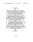
[0025] FIG. 1 is a flow chart illustrating a method of etching a Mo-based metal gate stack with an aluminium nitride barrier according to one embodiment of the present invention;
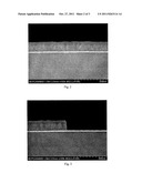
[0026] FIG. 2 shows an SEM photograph of the semiconductor structure after a MoAlN metal gate layer, an AlN barrier layer, a polysilicon gate layer and a hard mask of SiO2 are formed in sequence on a high K dielectric layer of HfSiAlON according to one embodiment of the present invention;
[0027] FIG. 3 shows an SEM photograph of the semiconductor structure after the polysilicon layer is etched with an optimized etching process using the hard mask according to one embodiment of the present invention; and
[0028] FIG. 4 shows an SEM photograph of the semiconductor structure after a stacked structure including an AlN barrier layer, a MoAlN metal gate layer and a high K dielectric layer is etched using a BCl3/O2/Ar etching gas according to one embodiment of the present invention.
DETAILED DESCRIPTION OF PREFERRED EMBODIMENTS
[0029] The invention will be further illustrated in detail in the following embodiments in conjunction with the accompanying drawings, so that the object, solution and advantages of the present invention are more apparent.
[0030] FIG. 1 is a flow chart illustrating a method of etching a Mo-based metal gate stack with an aluminium nitride barrier according to the present invention. The method comprises the following steps:
[0031] forming a SiO2 layer, a high K dielectric layer, a Mo-based metal gate layer, an AlN barrier layer, a silicon gate layer and a hard mask in sequence on a semiconductor substrate;
[0032] performing lithography on the semiconductor substrate with the SiO2 interface layer, the high K dielectric layer, the Mo-based metal gate layer, the AlN barrier layer, the silicon gate layer and the hard mask, and etching the hard mask;
[0033] removing the photoresist, and performing an anisotropic etching for silicon gate with high selectivity by dry etching using the hard mask;
[0034] performing an anisotropic etching for the AlN barrier layer, the Mo-based metal gate layer, and the high K dielectric layer by a dry etching.
[0035] In the above method, the high K dielectric layer is made of one selected from the group consisting of HfO2, HfON, HfAlO, HfAlON, HfTaO, HfTaON, HfSiO, HfSiON, HfLaO and HfLaON. The Mo-based metal gate layer is made of one selected from the group consisting of Mo, MoN, MoAlN and a stacked structure having any two of them; The AlN barrier layer is formed by a physical vapor deposition and having a thickness of about 2-10 nm. The silicon gate layer is made of polysilicon or amorphous silicon. The hard mask is made of one selected from the group consisting of silicon oxide, silicon nitride and a stacked structure of them.
[0036] The step of performing an anisotropic etching for the AlN barrier layer, the Mo-based metal gate layer, and the high K dielectric layer by a dry etching is an is anisotropic and highly selective etching for the AlN barrier layer, the Mo-based metal gate layer, and the high K dielectric layer using a BCl3-based etching gas. The BCl3-based etching gas comprises one or more selected from the group consisting of Cl2, O2, and Ar, in addition to BCl3. The BCl3-based etching gas has a ratio of Cl2:BCl3=0˜1:4, a ratio of O2:BCl3=0˜1:8, and a ratio of Ar:BCl3=1:5 to 1:2.
[0037] The dry etching for a stacked structure of the AlN barrier layer, the Mo-based metal gate and the high K dielectric layer is performed under the conditions of a top electrode power of about 140˜450 W, a bottom electrode power of about 30˜120 W, a chamber pressure of about 4˜15 mtorr, a total flow rate of the BCl3-based etching gas of about 50˜130 sccm, and a temperature of the chamber and the electrodes of about 50˜80° C.
[0038] FIGS. 2 to 4 show the semiconductor structure at various stages of the method for etching the Mo-based metal gate stack with the aluminium nitride barrier according to one embodiment of the present invention, corresponding to the flow chart shown in FIG. 1.
[0039] FIG. 2 shows an SEM photograph of the semiconductor structure after a MoAlN metal gate layer, an AlN barrier layer, a polysilicon gate layer and a hard mask of SiO2 are formed in sequence on a high K dielectric layer of HfSiAlON according to one embodiment of the present invention. The semiconductor structure in FIG. 2 is formed with the following steps: forming a SiO2 interface layer on a Si substrate by a rapid thermal oxidation (RTO); forming a high K dielectric layer of HfSiAlON with a thickness of about 3 nm by a physical vapor deposition; performing a high-temperature treatment at about 900° C.; forming a MoAlN metal gate with a thickness of about 14 nm by a physical vapor deposition; depositing an AlN barrier layer with a thickness of about 5.0 nm in situ; forming a polysilicon layer with a thickness of about 110 nm by a low-pressure chemical vapor deposition; and forming a SiO2 hard mask with a thickness of about 65 nm by a low-temperature thermal oxidation. As shown in FIG. 2, the stacked structure with a metal gate inserted between a high-k dielectric and polysilicon after the barrier layer is added has an improved thermal stability, and meets the requirement of manufacturing a semiconductor device.
[0040] FIG. 3 shows an SEM photograph of the semiconductor structure after the polysilicon layer is etched with an optimized etching process using the hard mask according to the present invention. The semiconductor structure in FIG. 3 is formed with the following steps: performing lithography on the semiconductor substrate with the SiO2 interface layer, the high K dielectric layer, the Mo-based metal gate layer, the AlN barrier layer, the silicon gate layer and the hard mask using a photoresist, and etching the hard mask; removing the photoresist, and then performing an anisotropic etching for silicon gate with high selectivity by dry etching using the hard mask. As shown in FIG. 3, the etching provides a steep etching profile of polysilicon and has a high selectivity with respect to the underlying barrier layer.
[0041] FIG. 4 shows an SEM photograph of the semiconductor structure after a stacked structure including an AlN barrier layer, a MoAlN metal gate layer and a high K dielectric layer is etched using a BCl3/O2/Ar etching gas according to one embodiment of the present invention. The semiconductor structure in FIG. 4 is formed with the following steps after those shown in FIGS. 2 and 3: etching the hard mask and the silicon gate layer by a dry etching; then etching the stacked structure including the AlN barrier layer, the MoAlN metal gate layer and the high K dielectric layer with optimize conductions such as a mixture ratio of BCl3/Cl2/Ar etching gas, a top electrode power and a bottom electrode power, a chamber pressure, and a temperature of the chamber and the electrodes. As shown in FIG. 4, the etching process provides vertical etching profiles of polysilicon and metal gate layers and has no residue. Moreover, the etching causes little loss of Si substrate.
[0042] The present method for etching a Mo-based metal gate stack with an aluminium nitride barrier layer in a gate-first process meets the requirement of an integration of a high K dielectric/metal gate stack in a nano-scale CMOS device, which facilitates the integration of the high K dielectric/metal gate stack.
[0043] While the invention has been described with reference to specific embodiments, the description is illustrative of the invention and is not to be considered as limiting the invention. Various modifications and applications may occur for those skilled in the art without departing from the true spirit and scope of the invention as defined by the appended claims.
User Contributions:
Comment about this patent or add new information about this topic:
| People who visited this patent also read: | |
| Patent application number | Title |
|---|---|
| 20160056499 | PROCESS FOR FABRICATION OF ENHANCED "-ALUMINA SOLID ELECTROLYTES FOR ENERGY STORAGE DEVICES AND ENERGY APPLICATIONS |
| 20160056498 | METHODS OF FORMING BIOCOMPATIBLE RECHARGABLE ENERGIZATION ELEMENTS FOR BIOMEDICAL DEVICES |
| 20160056497 | BATTERY CELL OF VERTICALLY STACKED STRUCTURE |
| 20160056496 | METHODS TO FORM BIOCOMPATIBLE ENERGIZATION ELEMENTS FOR BIOMEDICAL DEVICES COMPRISING LAMINATES AND PLACED SEPARATORS |
| 20160056495 | ACCUMULATOR DEVICE |
Images included with this patent application:
 |  |
| New patent applications in this class: | |
| Date | Title |
|---|---|
| 2016-12-29 | Method for manufacturing semiconductor device having metal gate |
| 2016-12-29 | Multi-gate field effect transistors having oxygen-scavenged gate stack |
| 2016-09-01 | Co-fabrication of non-planar semiconductor devices having different threshold voltages |
| 2016-07-14 | Asymmetric high-k dielectric for reducing gate induced drain leakage |
| 2016-07-14 | Asymmetric high-k dielectric for reducing gate induced drain leakage |
| New patent applications from these inventors: | |
| Date | Title |
|---|---|
| 2017-06-01 | Subscription service for monitoring changes in remote content |
| 2017-06-01 | Readiness checker for content object movement |
| 2017-01-26 | Method, system, and computer program product to update content on networked cache servers |
| 2016-03-24 | Cmos device and method for manufacturing the same |
| 2016-03-03 | Biased esd circuit |
| Top Inventors for class "Semiconductor device manufacturing: process" | |
| Rank | Inventor's name |
|---|---|
| 1 | Shunpei Yamazaki |
| 2 | Shunpei Yamazaki |
| 3 | Kangguo Cheng |
| 4 | Chen-Hua Yu |
| 5 | Devendra K. Sadana |