Patent application title: SEMICONDUCTOR DEVICE AND METHOD FOR FABRICATING THE SAME
Inventors:
Weon-Chul Jeon (Ichon-Shi, KR)
Assignees:
Hynix Semiconductor Inc.
IPC8 Class: AH01L2978FI
USPC Class:
257330
Class name: Short channel insulated gate field effect transistor gate controls vertical charge flow portion of channel (e.g., vmos device) gate electrode in groove
Publication date: 2011-10-13
Patent application number: 20110248338
Abstract:
A semiconductor device includes a substrate where an isolation region and
an active region are defined, an anti-interference layer formed over the
substrate in the isolation region, and a gate line simultaneously
crossing the active region and the anti-interference layer.Claims:
1. A semiconductor device, comprising: a substrate defining an isolation
region and an active region; an anti-interference layer formed over the
substrate in the isolation region; and a gate line crossing the active
region and the anti-interference layer.
2. The semiconductor device of claim 1, wherein the anti-interference layer includes one selected from the group consisting of an oxide layer, a nitride layer, an oxynitride layer, a carbon (C) containing layer, and a combination thereof.
3. The semiconductor device of claim 1, wherein the anti-interference layer has a thickness of approximately 100 Å to approximately 1,000 Å.
4. The semiconductor device of claim 1, wherein the gate line further includes a recess structure.
5. The semiconductor device of claim 4, wherein the recess structure is of one selected from the group consisting of a polygon type, a bulb type, and a saddle type
6. The semiconductor device of claim 1, wherein the gate line includes: a gate insulation layer formed over the substrate; a gate conductive layer formed over the gate insulation layer and including a polysilicon layer; and a gate hard mask layer formed over the gate conductive layer.
7.-13. (canceled)
Description:
CROSS-REFERENCE TO RELATED APPLICATIONS
[0001] The present invention is a divisional of U.S. patent application Ser. No. 12/165,145, filed on Jun. 30, 2008, which claims priority of Korean patent application number 2007-0104068, filed on Oct. 16, 2007, both of which are incorporated by reference in their entirety.
BACKGROUND OF THE INVENTION
[0002] The present invention relates to a semiconductor device and a method for fabricating the same. More particularly, the present invention relates to a semiconductor device that reduces a passing gate effect and a method for fabricating the same.
[0003] As semiconductors become highly integrated, electric characteristics such as a threshold voltage and a refresh rate requires an increase when a channel dimension decreases. Thus, a recess gate structure is introduced to increase the channel length by selectively etching a substrate.
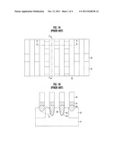
[0004] FIG. 1A illustrates a top view of a typical semiconductor device.
[0005] FIG. 1B illustrates a cross-sectional view of the semiconductor device shown in FIG. 1A cut along a line X-X'.
[0006] Referring to FIGS. 1A and 1B, a substrate 11 where isolation region and active region 13 are defined by an insulation layer 12 is selectively etched to form a recess pattern 14. A gate insulation layer 15 is formed over the recess pattern 14. Polysilicon layer 16, tungsten layer 17, and gate hard mask layer 18 are formed over a resultant structure including the recess pattern 14. Then, a patterning process is performed thereon to form gate lines GL. Thus, a plurality of gate lines GL are formed simultaneously crossing the isolation region and the active region 13. The gate lines GL crossing the active region 13 is called a main gate and the gate lines GL crossing the isolation region is called a passing gate.
[0007] However, as semiconductor devices become highly integrated, a physical gap between the main gate and the passing gate decreases. Thus, a threshold of the main gate changes and a parasitic capacitance between the main gate and the passing gate increases due to a bias applied to the passing gate. That is, the passing gate effect occurs.
[0008] Furthermore, a portion of the isolation layer 12 is etched during an etch process for forming the recess pattern 14 in the aforementioned typical method. Generally, the isolation layer 12 is etched down to approximately 2/3 to approximately 1/2 of the recess pattern 14. The damage of the isolation layer 12 decreases the physical gap between the main gate and the passing gate (refer to `A` area of FIG. 1B). Thus, the described passing effect becomes more intense.
SUMMARY OF THE INVENTION
[0009] Embodiments of the present invention relate to a semiconductor device reducing a passing gate effect and a method for fabricating the same. This invention increases a physical gap between a main gate and a passing gate to reduce the passing gate effect.
[0010] In accordance with an aspect of the present invention, there is provided a semiconductor device including a substrate where an isolation region and a plurality of active regions are defined, an anti-interference layer formed over the substrate in the isolation region, and a gate line simultaneously crossing the active region and the anti-interference layer.
[0011] In accordance with another aspect of the present invention, there is provided a method for fabricating a semiconductor device. The method includes forming an anti-interference pattern exposing a portion of a substrate in an active region over the substrate including an isolation region and an active region, forming a gate conductive layer over a resultant structure including the anti-interference pattern, forming a gate hard mask layer over the gate conductive layer, and selectively etching the gate hard mask layer, the gate conductive layer, and the anti-interference pattern to form a plurality of gate lines simultaneously crossing the isolation region and the active region.
BRIEF DESCRIPTION OF THE DRAWINGS
[0012] FIG. 1A illustrates a top view of a typical semiconductor device.
[0013] FIG. 1B illustrates a cross-sectional view of the semiconductor device shown in FIG. 1A cut along a line X-X'.
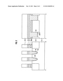
[0014] FIG. 2 illustrates a cross-sectional view of a semiconductor device in accordance with an embodiment of the present invention, the cross-sectional view oriented as shown in FIG. 1A cut along the line X-X'.
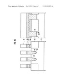
[0015] FIGS. 3A to 3C illustrate cross-sectional views describing a method for fabricating the semiconductor device in accordance with an embodiment of the present invention.
DESCRIPTION OF SPECIFIC EMBODIMENTS
[0016] Embodiments of the present invention relate to a semiconductor device for reducing a passing gate effect and a method for fabricating the same.
[0017] FIG. 2 illustrates a cross-sectional view of a semiconductor device in accordance with an embodiment of the present invention, the cross-sectional view oriented as shown in FIG. 1A cut along the line X-X'.
[0018] Referring to FIG. 2, the semiconductor device in this invention includes a substrate 21 where a plurality of active regions 23 are defined by an isolation region 22, an anti-interference layer 25A formed over the substrate 21, and a plurality of gate lines GL simultaneously crossing the active region 23 and the anti-interference layer 25A.
[0019] The anti-interference layer 25A increases a gap between a gate line crossing the active region 23 (i.e., a main gate) and a gate line crossing the isolation layer 22 (i.e., a passing gate), thereby reducing a passing gate effect. The anti-interference layer 25A may include any materials having an insulation characteristic and formed to have a thickness of approximately 100 Å to approximately 1,000 Å.
[0020] For instance, the anti-interference layer 25A may include one selected from the group consisting of an oxide layer, a nitride layer, an oxynitride layer, a carbon (C) containing layer, and a combination thereof. The oxide layer may include one of a silicon oxide (SiO2) layer, a boron phosphorus silicate glass (BPSG) layer, a phosphorus silicate glass (PSG) layer, a tetra ethyle ortho silicate (TEOS) layer, an un-doped silicate glass (USG) layer, a spin on glass (SOD) layer, a high density plasma (HDP) layer, and a spin on dielectric (SOD) layer. The nitride layer may include a silicon nitride (Si3N4) layer and the C containing layer may include an amorphous carbon layer (ACL) or a carbon rich polymer layer.
[0021] Although not shown, the anti-interference layer 25A may include a gate insulation layer formed between the passing gate and the substrate 21 in the isolation region 22.
[0022] The gate lines GL simultaneously crossing the active region 23 and the anti-interference layer 25A may further include a recess structure formed over the substrate 21 in the active region 23. The recess structure may be of a polygon type, a bulb type, or a saddle type. The bulb type indicates a recess structure having a wider lower portion than an upper portion thereof. Generally, the lower portion has a round type. The saddle type indicates a recess structure formed with a projection such as a fin at a bottom.
[0023] The gate lines GL may have a stack structure of a gate insulation layer 26, a first gate conductive layer 27, a second gate conductive layer 28, and a gate hard mask layer 29. The gate insulation layer 26 may include a silicon oxide layer. The first gate conductive layer 27 may include the gate insulation layer 26, e.g., the silicon oxide layer or a polysilicon layer having good interfere characteristic. The second gate conductive layer 28 may include one selected from the group consisting of a polysilicon layer, a metal layer (such as a tungsten layer or a nickel layer), a conductive metal nitride layer (such as a titanium nitride layer), a metal silicide layer (such as a tungsten silicide layer or a nickel silicide layer), and a combination thereof. The gate hard mask layer 29 may include one selected from the group consisting of an oxide layer, nitride layer, nitride oxide layer, C containing layer, and a combination thereof.
[0024] As described, the anti-interference layer 25A is formed over the substrate 21 in the isolation region 22 where the gate lines GL is crossed. Thus, the physical gap between the main gate and the passing gate increases to thereby reduce the passing gate effect.
[0025] FIGS. 3A to 3C illustrate cross-sectional views describing a method for fabricating the semiconductor device in accordance with an embodiment of the present invention.
[0026] Referring to FIG. 3A, a hard mask pattern including a pad oxide layer and a pad nitride layer is formed over the substrate 21. A trench is formed using the hard mask pattern as an etch barrier.
[0027] Sidewall oxide layer, liner nitride layer, and liner oxide layer are formed on a surface of the trench. Thus, an insulation layer for isolation is gap filled in the trench. The insulation layer for isolation may include an oxide layer, e.g. an HDP layer or a SOD layer.
[0028] The insulation layer for isolation layer is planarized to expose the pad nitride layer, and then the hard mask pattern is removed to form an isolation layer.
[0029] The region where the isolation layer is formed is referred to as an isolation region 22. The other region of the substrate 21 excluding the isolation region is not formed is referred as an active region 23. The anti-interference layer is deposited on the substrate 21 with the isolation region 22 and active region 23. The insulation layer for anti-interference may include one selected from the group consisting of an oxide layer, nitride layer, oxynitride layer, C containing layer, and a combination thereof.
[0030] The isolation layer for anti-interference decreases a gap between a subsequent main gate and passing gate. Thus, the physical gap between the main gate and the passing gate is increased to thereby reduce the passing gate effect. The isolation layer for anti-interference may also be used as an etch barrier during an etch process. When performing the etch process for forming the recess pattern, a portion of the insulation layer for anti-interference may be damaged. Thus, the insulation layer for anti-interference may have a thickness of more than approximately 100 Å, e.g., a thickness of approximately 100 Å to approximately 1,000 Å. An anti-interference pattern 25 is formed to expose a portion of the substrate 21 by selectively etching the insulation layer for anti-interference.
[0031] Referring to FIG. 3B, a recess pattern 24 is formed by etching the substrate 21 in the active region 23 using the anti-interference pattern 25 as an etch barrier.
[0032] The recess structure may be one selected from the group consisting of a polygon, a bulb type, and a saddle type.
[0033] A gate insulation layer 26 is formed over the substrate 21 in the active region 23 exposed by the anti-interference pattern 25. The gate insulation layer 26 can be formed through a thermal oxidation process and include a SiO2 layer.
[0034] A first gate conductive layer 27 is formed over a resultant structure including the gate insulation layer 26. The first gate conductive layer 27 may be a polysilicon layer having fine interface characteristic with the gate insulation layer 26, e.g., the silicon oxide layer.
[0035] The first gate conductive layer 27 is planarized to remove a height difference thereof formed by the anti-interference pattern 25. As a result, a first gate conductive pattern 27A is formed. The planarization process is performed using a chemical mechanical polishing (CMP) method.
[0036] Referring to FIG. 3c, a second gate conductive layer 28 is formed over the first gate conductive pattern 27A. The second gate conductive layer 28 may include one selected from the group consisting of a polysilicon layer, a metal layer (such as a tungsten layer or a nickel layer), a conductive metal nitride layer (such as a titanium nitride layer), a metal silicide layer such as a tungsten silicide layer or a nickel silicide layer, and a combination thereof.
[0037] A gate hard mask layer 29 is formed over the second gate conductive layer 28. The gate hard mask layer 29 may include one selected from the group consisting of an oxide layer, nitride layer, nitride oxide layer, C containing layer, and a combination thereof.
[0038] A hard mask pattern is formed over the gate hard mask layer 29. The gate hard mask layer 29, second gate conductive layer 28, first gate conductive pattern 27A, and anti-interference layer 25 are etched to form a plurality of gate lines simultaneously crossing the isolation region 22 and active region 23.
[0039] The gate line crossing the isolation region 22 includes the anti-interference pattern 25A formed over the substrate 21. That is, an anti-interference pattern 25A is formed between the passing gate and the substrate 21. The physical gap between the main gate and passing gate is increased. Thus, the passing gate effect is reduced.
[0040] In this invention, the gate line crossing the isolation region includes the anti-interference pattern formed over the substrate. Thus, the physical gap between the main gate and passing gate is increased and the passing gate effect is reduced.
[0041] While the present invention has been described with respect to the specific embodiments, the above embodiments of the present invention are illustrative and not limitative. It will be apparent to those skilled in the art that various changes and modifications may be made without departing from the spirit and scope of the invention as defined in the following claims.
User Contributions:
Comment about this patent or add new information about this topic:
| People who visited this patent also read: | |
| Patent application number | Title |
|---|---|
| 20140048188 | SWAPPABLE HANDLE SYSTEM FOR FASHION ACCESSORIES |
| 20140048187 | PROTECTIVE BAG FOR HANDBAG |
| 20140048186 | ALUMINUM ALLOY MATERIAL FOR USE IN THERMAL CONDUCTION APPLICATION |
| 20140048185 | METHOD OF HEAT TREATING A CAST IRON, IN PARTICULAR A NODULAR CAST IRON |
| 20140048184 | FINISH HEAT TREATMENT METHOD AND FINISH HEAT TREATMENT APPARATUS FOR IRON POWDER |
Images included with this patent application:
 |  |
 |  |
| Similar patent applications: | |
| Date | Title |
|---|---|
| 2008-09-04 | Semiconductor device and method for fabricating the same |
| 2008-09-11 | Semiconductor device and method of fabricating the same |
| 2008-09-18 | Semiconductor device and method for fabricating the same |
| 2008-09-18 | Semiconductor device and method for fabricating the same |
| 2008-09-18 | Semiconductor device and method for fabricating the same |
| New patent applications in this class: | |
| Date | Title |
|---|---|
| 2022-05-05 | Power semiconductor device |
| 2019-05-16 | Termination design for trench superjunction power mosfet |
| 2019-05-16 | Semiconductor device |
| 2019-05-16 | Semiconductor devices |
| 2018-01-25 | Semiconductor device and method of manufacturing the same |
| New patent applications from these inventors: | |
| Date | Title |
|---|---|
| 2009-04-16 | Semiconductor device and method for fabricating the same |
| 2008-11-27 | Semiconductor device and method for fabricating the same |
| Top Inventors for class "Active solid-state devices (e.g., transistors, solid-state diodes)" | |
| Rank | Inventor's name |
|---|---|
| 1 | Shunpei Yamazaki |
| 2 | Shunpei Yamazaki |
| 3 | Kangguo Cheng |
| 4 | Huilong Zhu |
| 5 | Chen-Hua Yu |