Patent application title: Rectifier driving circuit
Inventors:
Chao-Cheng Lu (Taipei, TW)
Chao-Cheng Lu (Taipei, TW)
IPC8 Class: AH02M7217FI
USPC Class:
363127
Class name: Using semiconductor-type converter in rectifier systems transistor
Publication date: 2011-04-07
Patent application number: 20110080760
Inventors list |
Agents list |
Assignees list |
List by place |
Classification tree browser |
Top 100 Inventors |
Top 100 Agents |
Top 100 Assignees |
Usenet FAQ Index |
Documents |
Other FAQs |
Patent application title: Rectifier driving circuit
Inventors:
Chao-Cheng Lu
Agents:
Assignees:
Origin: ,
IPC8 Class: AH02M7217FI
USPC Class:
Publication date: 04/07/2011
Patent application number: 20110080760
Abstract:
A rectifier driving circuit of the present invention, has a first driving
element and a second driving element, switching element comprises a FET,
a first driving element comprises the voltage drop resistor, a second
driving element comprises the series-connected circuit of the diodes, the
driving element for driving a FET, may be achieved rectify function.Claims:
1. A rectifier driving circuit, comprises: a first driving element for
voltage drop; a second driving element for driving gate-source of FET;
and a FET having no body diode and can be achieve rectify function.
2. A rectifier driving circuit as in claim 1, wherein: said a first and a second driving element comprises the series-connect circuit of resistor and diode
3. A rectifier driving circuit as in claim 1, wherein: said a first driving element comprise a resistor.
4. A rectifier driving circuit as in claim 1, wherein: said a second driving element comprises a diode.
5. A rectifier driving circuit as in claim 1, wherein: said a second driving element comprises the series-connect circuit of two diodes or more diodes.
6. A rectifier driving circuit as in claim 1, wherein: said a second driving element comprises series-connect circuit of diode and zener diode.
7. A rectifier driving circuit as in claim 1, wherein: said second terminal of a first driving element and first terminal of a second driving element connected together to said gate of the FET.
8. A rectifier driving circuit as in claim 1, wherein: said driving circuit comprises a first and a second driving element.
9. A rectifier driving circuit as in claim 8, wherein: said driving circuit connected to said first and second AC power source input terminal.
10. A rectifier driving circuit as in claim 1, wherein: said a FET of N-Channel type parallel to a diode; and P-junction node of said a diode connected to drain node of said a FET of N-Channel type, and N-junction node of said a diode connected to said source node of said a FET of N-Channel type.
11. A rectifier driving circuit as in claim 1, wherein: said a FET of P-Channel type parallel to a diode; and N-junction node of said a diode connected to drain node of said a FET of P-Channel type, and P-junction node of said a diode connected to said source node of said a FET of P-Channel type.
12. A rectifier driving circuit as in claim 1, wherein: said first terminal of a first driving element and said first terminal of a load connected together to said first AC power source input terminal; said second terminal of a first driving element and said first terminal of a second driving element connected together to said gate of N-Channel FET; said second terminal of a second driving element and said source of N-Channel FET connected together to said second AC power source in put terminal; and said drain of N-Channel FET connected to said second terminal of a load.
13. A rectifier driving circuit as in claim 1, wherein: said second terminal of a second driving element and said source of P-Channel FET connected together to said first AC power source input terminal; said first terminal of a second driving element and said second terminal of a first driving element connected together to said gate of P-Channel FET; said first terminal of a first driving element and said second terminal of a load connected together to second of AC power source input terminal; and said drain of P-Channel FET connected to said first terminal of a load.
Description:
BACKGROUND OF THE INVENTION
[0001] 1. Field of the Invention
[0002] The present invention related to a first driving element, a second driving element and an enhancement mode FET for rectifier driving circuit, especially FET there is not an intrinsic body diode can be achieve rectify function.
[0003] 2. Description of Related Arc
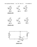
[0004] FIG. 7 shown a structures of the prior art half-wave rectifier. In this figure, FET F1 is responsible for rectification. In operation, when positive of AC power source in the terminal A, terminal B is negative, FET F1 turned on, FET F1 acts as a rectifier, the path of the current flow is from terminal A of AC power source though a load LD, FET F1 and back to terminal B; when negative of AC power source in the terminal A, terminal B is positive, FET F1 turned off, the path of the current flow is from terminal B of AC power source though intrinsic body diode DB of the FET F1, a load LD and back to terminal A, may be burnout by current of the prior art FET F1, and FET F1 having no responsible for rectification.
SUMMARY OF THE INVENTION
[0005] In order to provide a first driving element, a second driving element FET having no intrinsic body diode that may elevate the efficiency of half-wave rectifier, the present invention is proposed the following object:
[0006] The first object of the present invention provide a driving circuit for a rectifier, in which the rectifier simplicity is improved.
[0007] The second object of the present invention provide a diode parallel to the FET for surge current protection.
[0008] According to the defects of the prior art technology discussed above, a novel solution, the rectifier driving circuit is proposed in the present invention, which provides simplicity and for surge current protection in rectifier circuit.
BRIEF DESCRIPTION OF THE DRAWINGS
[0009] FIG. 1 shown the structures of a prior art N-Channel FET.
[0010] FIG. 2 shown the structures a having no intrinsic body diode N-Channel FET.
[0011] FIG. 3 shown the structures of a diode parallel to the N-Channel FET, a P-junction of the diode connected to drain of the N-Channel FET, a N-junction of the diode connected to source of the N-Channel FET.
[0012] FIG. 4 shown the structures of a prior art P-Channel FET.
[0013] FIG. 5 shown the structures a having no intrinsic body diode P-Channel FET.
[0014] FIG. 6 shown the structures of a diode parallel to the P-Channel FET, a N-junction of the diode connected to drain of the P-Channel FET, a P-junction of the diode connected to source of the P-Channel FET.
[0015] FIG. 7 is a circuit diagram of a prior art N-Channel FET for half-wave rectifier circuit.
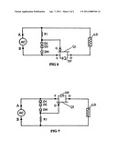
[0016] FIG. 8 is a circuit diagram of a first embodiment of the present invention.
[0017] FIG. 9 is a circuit diagram of a second embodiment of the present invention.
DETAILED DESCRIPTION OF THE PREFERRED EMBODIMENTS
[0018] FIG. 1 shows the structures of a prior art N-Channel FET, a N-junction of the intrinsic body diode DB connected to drain of the prior art N-Channel FET, a P-junction of the intrinsic body diode DB connected to source of the prior art N-Channel FET.
[0019] FIG. 2 shows the structures of a N-Channel FET having no intrinsic body diode, has a enhancement mode FET.
[0020] FIG. 3 shows the structures of a diode parallel to the N-Channel FET, a diode parallel to the N-Channel FET for surge current protection in the rectify circuit.
[0021] FIG. 4 shows the structures of a prior art P-Channel FET, a P-junction of the intrinsic body diode DB connected to drain of the prior art P-Channel FET, a N-junction of the intrinsic body diode DB connected to source of the prior art P-Channel FET.
[0022] FIG. 5 shows the structures of a P-Channel FET having no intrinsic body diode, has a enhancement mode FET.
[0023] FIG. 6 shows the structures of a diode parallel to the P-Channel FET, a diode parallel to the P-Channel FET for surge current protection in the rectify circuit.
[0024] As shown in FIG. 8, has a AC power source input terminal, a first terminal A and second terminal B of the input terminal, a N-Channel FET Q1, a first driving element R1, a second driving element D1, D2 . . . DN, and a load LD.
[0025] A inrush diode DP parallel to the N-Channel FET Q1 shown in FIG. 8, a driving circuit comprises a voltage drop resistor R1 and a diode D1 or series-connected with D1, D2 . . . DN diodes; the P-junction of D1, D2 . . . DN diodes connected to gate of the N-Channel PET Q1, the N-junction of D1, D2 . . . DN diodes connected to source of the N-Channel FET Q1, the driving voltage is equal to the forward voltage of series-connected of D1, D2 . . . DN diodes.
[0026] As shown in FIG. 8, when positive of AC power source in the terminal A, terminal B is negative, the P-junction is positive of the series-connected D1, D2 . . . DN diodes, the N-junction is negative of the series-connected of D1, D2 . . . DN diodes, the N-Channel FET Q1 is turned on, the driving voltage is equal to the forward voltage of series-connected of D1, D2 . . . DN diodes, the path of the current flows is from terminal A of the AC power source though a load LD, a N-Channel FET Q1, and back to terminal B of the AC power source.
[0027] As shown in FIG. 8, when negative of AC power source in the terminal A, terminal B is positive, the P-junction is negative of the series-connected of D1, D2 . . . DN diodes, the N-junction is positive of the series-connected of D1, D2 . . . DN diodes, the N-Channel FET Q1 is turned off, the rectifier is open circuit.
[0028] As shown in FIG. 9, has a AC power source input terminal, a first terminal A and second terminal B of the input terminal, a P-Channel FET Q2, a first driving element R1, a second driving element D1 . . . DN, and a load LD.
[0029] A surge diode DP parallel to the P-Channel FET shown in FIG. 9, a driving circuit comprises a voltage drop resistor R1 and a diode D1 or series-connected with D1, D2 . . . DN diodes; the N-junction of D1, D2 . . . DN diodes connected to gate of the P-Channel PET Q2, the P-junction of D1, D2 . . . DN diodes connected to source of the P-Channel PET Q2, the driving voltage is equal to the forward voltage of series-connected of D1, D2 . . . DN diodes.
[0030] As shown in FIG. 9, when positive of AC power source in the terminal A, terminal B is negative, the P-junction of the diode D1 is positive of the series-connected D1, D2 . . . DN diodes, the N-junction of the diode DN is negative of the series-connected of D1, D2 . . . DN diodes, the P-Channel FET Q2 is turned on, the driving voltage is equal to the forward voltage of series-connected of D1, D2 . . . DN diodes, the path of the current flows is from terminal A of the AC power source though a P-Channel FET Q2, a load LD, and back to terminal B of the AC power source.
[0031] As shown in FIG. 9, when negative of AC power source in the terminal A, terminal B is positive, the P-junction is negative of the diode D1 of the series-connected of D1, D2 . . . DN diodes, the N-junction of the diode DN is positive of the series-connected of D1, D2 . . . DN diodes, the P-Channel FET Q2 is turned off, the rectifier is open circuit.
[0032] The operation principle of the second driving element D1, D2 . . . DN of FIG. 8 and the second driving element D1, D2 . . . DN of FIG. 9 is same, both of the second driving element can be use a series-connected circuit of diode and zener diode replace, the driving voltage is equal to the forward voltage of diode and zener voltage of zener.
User Contributions:
comments("1"); ?> comment_form("1"); ?>Inventors list |
Agents list |
Assignees list |
List by place |
Classification tree browser |
Top 100 Inventors |
Top 100 Agents |
Top 100 Assignees |
Usenet FAQ Index |
Documents |
Other FAQs |
User Contributions:
Comment about this patent or add new information about this topic:
Images included with this patent application:
 |  |
 |
| New patent applications in this class: | |
| Date | Title |
|---|---|
| 2016-12-29 | Rectifier circuit including a self-clamping transistor |
| 2016-07-14 | Variable-voltage self-synchronizing rectifier circuits, methods, and systems |
| 2016-07-07 | Power conversion apparatus |
| 2016-06-23 | Transformer |
| 2016-06-16 | Layout of power converter |
| New patent applications from these inventors: | |
| Date | Title |
|---|---|
| 2022-08-25 | Method for using semiconductor intelligence line |
| 2016-03-10 | Universal cell |
| 2013-09-19 | Hall effect transformer |
| 2013-03-28 | Cell parallel device |
| 2013-02-21 | Switch |
| Top Inventors for class "Electric power conversion systems" | |
| Rank | Inventor's name |
|---|---|
| 1 | Ta-Yung Yang |
| 2 | Lieyi Fang |
| 3 | Alex B. Djenguerian |
| 4 | Martin Fornage |
| 5 | Balu Balakrishnan |