Patent application title: LAMINATED SUBSTRATE FOR AN INTEGRATED CIRCUIT BGA PACKAGE AND PRINTED CIRCUIT BOARDS
Inventors:
Nedyalko Slavov (Zurich, CH)
Nedyalko Slavov (Zurich, CH)
Heinz-Peter Wirtz (Dottingen, CH)
Kwei-Kuan Kuo (Zurich, CH)
Assignees:
ST-Ericsson SA
IPC8 Class: AH05K116FI
USPC Class:
174260
Class name: Conduits, cables or conductors preformed panel circuit arrangement (e.g., printed circuit) with electrical device
Publication date: 2011-03-17
Patent application number: 20110061917
Inventors list |
Agents list |
Assignees list |
List by place |
Classification tree browser |
Top 100 Inventors |
Top 100 Agents |
Top 100 Assignees |
Usenet FAQ Index |
Documents |
Other FAQs |
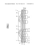
Patent application title: LAMINATED SUBSTRATE FOR AN INTEGRATED CIRCUIT BGA PACKAGE AND PRINTED CIRCUIT BOARDS
Inventors:
Nedyalko Slavov
Heinz-Peter Wirtz
Kwei-Kuan Kuo
Agents:
Assignees:
Origin: ,
IPC8 Class: AH05K116FI
USPC Class:
Publication date: 03/17/2011
Patent application number: 20110061917
Abstract:
A laminated substrate for an integrated circuit package, including a core
layer and at least one build-up layer located above only one side of said
core layer. An integrated circuit package, including a laminated
substrate and including an integrated circuit die placed above the side
build-up layer.Claims:
1. A laminated substrate for an integrated circuit package, comprising a
core layer and a build-up layer located above only one side of said core
layer.
2. A laminated substrate according to claim 1, including an electrical connection network comprising an electrical connection pattern on an external face of the core layer for an electrical connection of the connection network externally to the substrate.
3. A laminated substrate according to claim 1, including an electrical connection network connecting connection patterns of sides of the substrate through the core layer and the build-up layer.
4. A laminated substrate according to claim 1, including an electrical connection network that includes:an external connection pattern formed on an external side of the build-up layer,an intermediate connection pattern formed between the core layer and the build-up layer,first connection vias through the build-up layer, andsecond connection vias through drilled holes of the core layer.
5. A laminated substrate according to claim 1, in which the core layer includes a main layer and a sub-layer joined side by side.
6. A laminated substrate according to claim 5, in which the core layer includes a compensating layer integrated between the main layer and the sub-layer.
7. An integrated circuit package, comprising:an integrated circuit die; anda laminated substrate that includes a core layer and a build-up layer located above only one side of said core layer, the integrated circuit die being placed above the build-up layer.
8. An integrated circuit package according to claim 7, further comprising an electrical connection network coupled to the integrated circuit die.
9. A method, comprising:fabricating a laminated substrate for an integrated circuit package, the fabricating including forming a build-up layer above only one side of a thick core layer.
10. A method, comprising:fabricating a laminated substrate for an integrated circuit package, the fabricating including:forming connection layers on sides of a thick core layer,drilling mechanically holes through the core layer,realizing first connectors configured to connect said connection layers through the holes, andforming a build-up layer above only one side of said core layer and realizing second connectors on and through the build-up layer.
Description:
BACKGROUND
[0001]1. Technical Field
[0002]The present invention relates to the field of laminated substrates for integrated circuit packages.
[0003]2. Description of the Related Art
[0004]Currently, laminated substrates comprise multilayer symmetrical structures having thin build-up layers of equal thicknesses, integrating a connection network.
BRIEF SUMMARY
[0005]It is proposed a laminated substrate for an integrated circuit package.
[0006]The laminated substrate can include a core layer and at least one build-up layer located above only one side of said core layer.
[0007]The laminated substrate can include an electrical connection network comprising an electrical connection pattern on the external face of the core layer for an electrical connection of the network externally to the substrate.
[0008]The laminated substrate can include an electrical connection network connecting connection patterns of the sides of the substrate through the core layer and the at least one build-up layer.
[0009]The laminated substrate can include an electrical connection network comprising an external connection pattern formed on an external side of a build-up layer, at least one intermediate connection pattern formed between the core layer and the at least one build-up layer, vias through the at least one build-up layer and vias through drilled holes of the core layer.
[0010]The core layer can include a main layer and at least one sub-layer joined side by side.
[0011]The core layer can include at least one compensating layer integrated between the main layer and the sub-layer.
[0012]It is proposed an integrated circuit package, including a laminated substrate and including an integrated circuit die placed above the unique side build-up layer.
[0013]It is proposed an integrated circuit package, including a laminated substrate comprising a core layer, at least one build-up layer located above only one side of said core layer and an electrical connection network and including an integrated circuit die placed above a side build-up layer and connected to the connection network.
[0014]It is proposed a method for fabricating a laminated substrate for an integrated circuit package, comprising taking a thick core layer and forming at least one build-up layer above only one side of said core layer
[0015]It is proposed a method for fabricating a laminated substrate for an integrated circuit package, comprising taking a thick core layer, forming connection means on the sides of the core layer, drilling mechanically holes through the core layer and realizing connection means for connecting said connection patterns through the holes, and forming at least one build-up layer above only one side of said core layer and realizing connection means on and through the at least one build-up layer.
BRIEF DESCRIPTION OF THE SEVERAL VIEWS OF THE DRAWINGS
[0016]Other advantages and features will become apparent by studying integrated circuit device or package, described by way of non-limited examples and illustrated by the appended drawings in which:
[0017]FIG. 1 represents a cross section of an integrated circuit device or package,
[0018]FIG. 2 represents a cross section of an intermediate step of fabrication of a laminated substrate of FIG. 1;
[0019]FIG. 3 represents a cross section of another intermediate step of fabrication of a laminated substrate of FIG. 1;
[0020]FIG. 4 represents a cross section of another intermediate step of fabrication of a laminated substrate of FIG. 1;
[0021]FIG. 5 represents a cross section of an intermediate step of fabrication of a laminated substrate of FIG. 1;
[0022]FIG. 6 represents a cross section of another intermediate step of fabrication of a laminated substrate of FIG. 1;
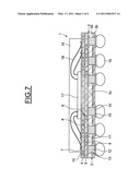
[0023]FIG. 7 represents a cross section of a variant of the laminated substrate of FIG. 1, with a compensating layer; and
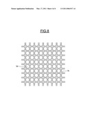
[0024]FIG. 8 represents a front view of a compensating layer.
DETAILED DESCRIPTION
[0025]Referring to FIG. 1, an integrated circuit package 1 is represented.
[0026]The integrated circuit package 1 includes a laminated substrate 2 which comprises a dielectric core layer 3 and comprises, only above one side of the core layer 3, a side dielectric build-up layer 4 and eventually at least an intermediate dielectric build-up layer 5 located between the core layer 3 and the side build-up layer 4.
[0027]It means that the other side of the core layer 3 is free from any build-up layer.
[0028]The laminated substrate 2 includes a metal electrical connection network 6.
[0029]The connection network 6 includes an external connection pattern 7 formed on the external side of the side build-up layer 4, an intermediate connection pattern 8 formed between the unique side build-up layer 4 and the intermediate build-up layer 5, an intermediate connection pattern 9 formed between the intermediate build-up layer 5 and the core layer 3.
[0030]The connection network 6 includes also vias 10 realized through the side build-up layer 4 for connecting the external connection pattern 7 to the intermediate connection pattern 8, vias 11 realized through the intermediate build-up layer 5 for connecting the intermediate connection patterns 8 and 9, and vias 12 realized through drilled hole 13 of the core layer 3 connected to the intermediate connection pattern 9, the external faces of the vias 12 forming an electrical connection pattern 14 of the external face of the core layer 3 for an electrical connection of the network 6 externally to the substrate 2.
[0031]The electrical connection pattern 14 can further comprise pads 15 formed on the external face of the core layer 3, adapted for receiving external connection balls 16.
[0032]The integrated circuit package 1 can include an integrated circuit die 17 which is linked to the external side of the side build-up layer 4, for example by means of a layer of glue.
[0033]The integrated circuit die 17 can be electrically connected to the external connection pattern 7 of the laminated substrate 2 by means of connection bond wires 18.
[0034]The integrated circuit package 1 can include also an encapsulating block 19 which encapsulates the die 17 and the connection wires 18 above the external face of the side build-up layer 4, for example by molding.
[0035]The core layer 3 can be of a one-piece. But, the core layer 3 can comprises a main layer 3a and at least one sub-layer 3b joined side by side, the at least one sub-layer 3b being opposite to the build-up layers 4 and 5. Furthermore, as illustrated on FIGS. 7 and 8, the core layer 3 can includes at least one compensating layer 3c integrated between the main layer 3a and the at least one sub-layer 3b and or integrated between sub-layers 3b. The compensating layer 3c can be formed as a dummy metal pattern having gaps 3d through which the drilled holes 13 are done at a distance for having no contact between the metal pattern and the vias 12.
[0036]The at least one sub-layer 3b and/or the at least one compensating layer 3c can be chosen in such way that they match the mechanical and the thermal properties of the upper-sided build-up layers 4 and 5 in order to avoid a possible warp of the laminated substrate 2 during a thermal stress.
[0037]Other features and advantageous of the laminated substrate 2 and the complete integrated circuit package 1 will be now indicated.
[0038]The proposed structures are able to achieve a performed combination of mechanical resistances, electrical connections and adapted methods of fabrication.
[0039]Comparatively, the thickness of the core layer 3 is sufficiently higher than the thickness of the build-up layer 4 and 5 such that the laminated substrate 2 is asymmetrical, the core layer 3 being thick and the build-up layers 4 and 5 being thin.
[0040]So, the core layer can ensure a great part of the mechanical resistance and the strength of the substrate and consequently the mechanical resistance and the strength of the package.
[0041]The mechanical and thermal properties of the core layer can be chosen in such a way that they compensate these properties of the build-up layers.
[0042]Specific methods of fabrication can be used on one hand for the core layer and on the other hand for the build-up layers.
[0043]The build-up layers are able to result of advanced methods of fabrication for achieving dense interconnections, as laser drills, dry films and etching of high precision for having fine pattern formation. So, the build-up layers can be used for very high routings and most of the routings.
[0044]The core layer can ensure direct connections towards and from external components, which necessitate generally limited amount of signals and does not need very high routing resolution. So, classic methods of fabrication can be used, as mechanical drills, chemical deposition and etching.
[0045]For example, the laminated substrate 2 can be fabricated as following.
[0046]Having a core layer plate 3, metal layers are laminated on the sides of the core layer 3 and are etching to form desired metal connection pattern means corresponding substantially to the connection patterns 9 and 14 (FIG. 2).
[0047]After that, the core layer plate 3 is drilled mechanically for obtaining holes 13 (FIG. 3).
[0048]After that, metal plating is realized for obtaining vias 12 through the holes 13, which connect the connection patterns 9 and 14 (FIG. 4).
[0049]After having filled the holes 13 with epoxy material, a build-up layer 5 and a metal layer 20 are laminated only on the side of the core layer 3 having the connection patterns 9 (FIG. 5).
[0050]After that, by means of laser drilling and etching method, an intermediate connection pattern 8 and vias 11 are realized in the metal layer 20 and through the build-up layer 5 for being connected to the connection pattern 9 (FIG. 6).
[0051]The above steps (FIGS. 5 and 6) can be repeated for forming the side built-up layer 4, the side connection pattern 7 and the vias 10. An additional step can be operated for forming the external connection pads 15.
[0052]Although embodiments of the devices and systems of the present disclosure have been illustrated in the accompanying drawings and described in the foregoing detailed description, it will be understood that the invention is not limited to the embodiments disclosed, but is capable of numerous rearrangements, modifications and substitutions without departing from the spirit of the disclosure.
[0053]The various embodiments described above can be combined to provide further embodiments. These and other changes can be made to the embodiments in light of the above-detailed description. In general, in the following claims, the terms used should not be construed to limit the claims to the specific embodiments disclosed in the specification and the claims, but should be construed to include all possible embodiments along with the full scope of equivalents to which such claims are entitled. Accordingly, the claims are not limited by the disclosure.
User Contributions:
comments("1"); ?> comment_form("1"); ?>Inventors list |
Agents list |
Assignees list |
List by place |
Classification tree browser |
Top 100 Inventors |
Top 100 Agents |
Top 100 Assignees |
Usenet FAQ Index |
Documents |
Other FAQs |
User Contributions:
Comment about this patent or add new information about this topic:
Images included with this patent application:
 |  |
 |  |
 |
| New patent applications in this class: | |
| Date | Title |
|---|---|
| 2022-05-05 | Electronic device and manufacturing method thereof |
| 2019-05-16 | Thin film capacitors for core and adjacent build up layers |
| 2019-05-16 | Galvanic isolation for isolation transformer |
| 2019-05-16 | Multilayer electronic component and board having the same |
| 2019-05-16 | Electronic component and electronic component mounting circuit board |
| New patent applications from these inventors: | |
| Date | Title |
|---|---|
| 2020-03-19 | Semiconductor device with encapsulant deposited along sides and surface edge of semiconductor die in embedded wlcsp |
| 2014-04-03 | Semiconductor device and method of depositing encapsulant along sides and surface edge of semiconductor die in embedded wlcsp |
| 2014-04-03 | Semiconductor device and method of using a standardized carrier in semiconductor packaging |
| 2013-10-31 | Interfacing a switch array |
| 2013-08-15 | Packaging an integrated circuit die |
| Top Inventors for class "Electricity: conductors and insulators" | |
| Rank | Inventor's name |
|---|---|
| 1 | Douglas B. Gundel |
| 2 | Shou-Kuo Hsu |
| 3 | Michimasa Takahashi |
| 4 | Hideyuki Kikuchi |
| 5 | Tsung-Yuan Chen |