Patent application title: SERIAL LINK BUFFER FILL-LEVEL COMPENSATION USING MULTI-PURPOSE START OF PROTOCOL DATA UNIT TIMING CHARACTERS
Inventors:
Mark Megarity (Ottawa, CA)
Assignees:
ALCATEL LUCENT
IPC8 Class: AG06F514FI
USPC Class:
710 53
Class name: Input/output data processing input/output data buffering alternately filling or emptying buffers
Publication date: 2009-11-05
Patent application number: 20090276550
Inventors list |
Agents list |
Assignees list |
List by place |
Classification tree browser |
Top 100 Inventors |
Top 100 Agents |
Top 100 Assignees |
Usenet FAQ Index |
Documents |
Other FAQs |
Patent application title: SERIAL LINK BUFFER FILL-LEVEL COMPENSATION USING MULTI-PURPOSE START OF PROTOCOL DATA UNIT TIMING CHARACTERS
Inventors:
Mark Megarity
Agents:
Kramer & Amado, P.C.
Assignees:
ALCATEL LUCENT
Origin: ALEXANDRIA, VA US
IPC8 Class: AG06F514FI
USPC Class:
710 53
Patent application number: 20090276550
Abstract:
Embodiments of the invention provide improved timing compensation for a
bidirectional serial link in order to relax accuracy requirements of
clock sources used for the link. Fill levels of receiver buffers at
either ends of the link are used to determine a particular type of start
of PDU (SOP) character sequence to use when forming a PDU for
transmission over the link. When a given type of SOP character sequence
is present in a PDU received at one end of the link, a next PDU to be
transmitted from the same end of the link is delayed by a predetermined
amount of time to allow the receiver buffer at the other end of the link
to decrease its fill level before receiving the next PDU.Claims:
1. A circuit card for communicating protocol data units PDUs over a
bidirectional serial link that includes a first unidirectional serial
link for communicating PDUs in one direction and a second unidirectional
serial link for communicating PDUs in an opposite direction, the circuit
card comprising:a transmitter module for transmitting PDUs over the first
unidirectional serial link;a receiver module for receiving PDUs from the
second unidirectional serial link; anda control link coupling the
receiver module to the transmitter module for conveying control
indications from the receiver module to the transmitter module.
2. The circuit card of claim 1, wherein:the receiver module includes a receiver buffer for storing PDUs received from the second unidirectional serial link and is operable to determine and send a particular control indication to the transmitter module, the determination depending upon a relationship between a fill level of the receiver buffer and a threshold; andthe transmitter module is operable to determine and use a particular start of PDU SOP character sequence to form a next PDU to be transmitted over the first unidirectional serial link, the determination depending upon the particular control indication received from the receiver module.
3. The circuit card of claim 2, wherein:the receiver module is further operable to send a first control indication as the particular control indication to the transmitter module responsive to the fill level being below the threshold; andthe transmitter module is further operable use a first SOP character sequence as the particular SOP character sequence responsive to receiving the first control indication as the particular control indication.
4. The circuit card of claim 3, wherein:the receiver module is further operable to send a second control indication as the particular control indication to the transmitter module responsive to the fill level being above the threshold; andthe transmitter module is further operable use a second SOP character sequence as the particular SOP character sequence responsive to receiving the second control indication as the particular control indication.
5. The circuit card of claim 1, wherein the receiver module is operable to determine and send a particular control indication to the transmitter module responsive to receiving a first PDU from the second unidirectional serial link, the determination being dependent upon a start of PDU SOP character sequence of the first PDU.
6. The circuit card of claim 5, wherein:the receiver module is further operable to send a third control indication as the particular control indication to the transmitter module responsive to the first PDU starting with a particular SOP character sequence; andthe transmitter module is operable to delay transmission of the next PDU by a predetermined amount of time responsive to receiving the third control indication from the receiver module.
7. The circuit card of claim 6, wherein the predetermined amount of time is an amount of time taken to transmit one character on the first unidirectional serial link.
8. The circuit card of claim 2, wherein:the determination of the receiver module is dependent upon an SOP character sequence of a first PDU received from the second unidirectional serial link; andthe transmitter module is further operable to delay transmission of the next PDU by a predetermined amount of time depending upon the particular control indication received from the receiver module.
9. The circuit card of claim 8, wherein the predetermined amount of time is an amount of time taken to transmit one character on the first unidirectional serial link.
10. A receiver module for receiving protocol data units PDUs from unidirectional serial link, comprising:an input for connecting to the unidirectional serial link;an output for coupling to a transmitter module; anda receiver buffer for storing PDUs received from the unidirectional serial link,wherein the receiver module is operable to determine and send a particular control indication to the transmitter module, the determination depending upon a relationship between a fill level of the receiver buffer and a threshold.
11. The receiver module of claim 10, wherein the receiver module is further operable to determine and send another control indication to the transmitter module responsive to receiving a PDU from the unidirectional serial link, the determination being dependent upon a start of PDU SOP character sequence of the PDU.
12. A transmitter module for transmitting protocol data units PDUs on a unidirectional serial link, comprising:an output for connecting to the unidirectional serial link; andan input for coupling to a receiver module,wherein the transmitter module is operable to determine and use a particular start of PDU SOP character sequence to form a next PDU to be transmitted over the unidirectional serial link, the determination depending upon a particular control indication received from the receiver module.
13. The transmitter module of claim 12, wherein the transmitter module is further operable to delay transmission of the next PDU by a predetermined amount of time responsive to receiving another control indication from the receiver module.
14. A transceiver module for transmitting and receiving protocol data units PDUs over a bidirectional serial link that includes a first unidirectional serial link for communicating PDUs in one direction and a second unidirectional serial link for communicating PDUs in an opposite direction, the transceiver module comprising:an output for connecting to the first unidirectional serial link;an input for connecting to the second unidirectional serial link; anda receiver buffer for storing PDUs received from the second unidirectional serial link,wherein the transceiver module is operable to determine and use a particular start of PDU SOP character sequence to form a next PDU to be transmitted over the first unidirectional serial link, the determination depending upon a relationship between a fill level of the receiver buffer and a threshold.
15. The transceiver module of claim 14, wherein the transceiver module is further operable to delay transmission of the next PDU by a predetermined amount of time responsive to receiving a PDU from the second unidirectional serial link, the determination being dependent upon an SOP character sequence of the PDU received from the second unidirectional serial link.
16. A circuit card for transmitting and receiving protocol data units PDUs over a bidirectional serial link that includes a first unidirectional serial link for communicating PDUs in one direction and a second unidirectional serial link for communicating PDUs in an opposite direction, the circuit card comprising:an output for connecting to the first unidirectional serial link;an input for connecting to the second unidirectional serial link; anda receiver buffer for storing PDUs received from the second unidirectional serial link,wherein the circuit card is operable to determine and use a particular start of PDU SOP character sequence to form a next PDU to be transmitted over the first unidirectional serial link, the determination depending upon a relationship between a fill level of the receiver buffer and a threshold.
17. The circuit card of claim 16, wherein the circuit card is further operable to delay transmission of the next PDU by a predetermined amount of time responsive to receiving a PDU from the second unidirectional serial link, the determination being dependent upon an SOP character sequence of the PDU received from the second unidirectional serial link.
18. A method of performing timing compensation on a bidirectional serial link that includes a first unidirectional serial link for communicating protocol data units PDUs in one direction and a second unidirectional serial link for communicating PDUs in an opposite direction, the method comprising the steps of:receiving a first PDU from the second unidirectional serial link;storing the first PDU in a receiver buffer;detecting a fill level of the receiver buffer;comparing the fill level to a threshold;determining a particular start of PDU SOP character sequence depending upon a relationship between the fill level and the threshold;forming a second PDU using the particular SOP character sequence; andtransmitting the second PDU onto the first unidirectional serial link.
19. The method of claim 18, wherein:the step of receiving comprises detecting an SOP character sequence of the first PDU and determining a type of the SOP character sequence; andthe step of transmitting comprises delaying transmission of the second PDU by a predetermined amount of time responsive to determining that the SOP character sequence is of a given type.
20. The method of claim 19, wherein the predetermined amount of time is an amount of time taken to transmit one character on the first unidirectional serial link.
Description:
FIELD OF THE INVENTION
[0001]The present invention is directed to data communication systems, in particular high speed data communication over a serial link.
BACKGROUND OF THE INVENTION
[0002]Data communications systems, and in general many other types of electronic systems, rely on a backplane based architecture comprising a plurality of circuit cards that plug into, or are otherwise electrically connected to, a system backplane. The system backplane is a facility over which the circuit cards can communicate with each other and over which power is supplied to the circuit cards. Examples of the type circuit cards included in data communications systems include control cards, input/output (I/O) cards, line cards, and processor cards.
[0003]A typical data communication system employs multiple serial links across the backplane for communications between the various circuit cards of the system. Generally, such communications occur over bidirectional serial links, each of which comprises a pair of unidirectional links each link of the pair being for data transmission in an opposite direction than the other link of the pair. A serial input/output (I/O) interface at each end of each bidirectional link comprises a transmitter and receiver. Typically both the transmitter and the receiver are implemented in one component known as a serializer/deserializer (SERDES). Generally, on any given unidirectional serial link, the transmitter at one end of the link is asynchronous to the receiver at the other end of that link. This is because transmitter and receiver each derive their timing from a respective reference clock, and those reference clocks are asynchronous to each other since they are typically generated locally at a respective circuit card.
[0004]A method exists to compensate for timing discrepancies in clocking of the transmitter and receiver at either end of a unidirectional serial link, but this method requires the use of clocks with known accuracies, which tends to make it costly to implement. Also, a requirement of the method is that the transmitter sends several special timing characters, known as idle or `stuff` characters, every predetermined interval of time so that the receiver can compensate for its receive buffer fill rate. Since the interval between the transmission of the special timing characters is fixed, as well as the number of special characters that are inserted, the accuracy required by a reference clock used by the method is dictated by this interval and sequence length of the special timing characters. This aspect of the method hinders the use of inexpensive clocking sources in systems employing the method. Furthermore, in-band insertion of idle characters for the unique purpose of timing compensation at the receiver consumes link bandwidth as overhead, and is therefore inefficient.
[0005]In view of the foregoing, it would be desirable to have a solution that allows more design freedom in the selection of serial link reference clock sources than is available using the aforementioned known timing compensation method.
SUMMARY OF THE INVENTION
[0006]Embodiments of the invention provide improved timing compensation for a serial link in order to relax accuracy requirements of clock sources used for the link.
[0007]Some embodiments of the invention enable a transmitter at a near-end of a bidirectional serial link to forward a near-end fill level indication of a receiver buffer at the same end of the link to a receiver at a far-end of the link, which indication is used by a transmitter at the far-end of the link to adjust its data transmission rate.
[0008]Additionally, some embodiments of the invention also likewise provide, to the near-end transmitter, a far-end indication of a fill level of a receiver buffer at the far-end of the bidirectional link, thereby enabling the near-end transmitter to adjust its data transmission rate accordingly.
[0009]This communication of the near-end and far-end fill level indications represents real-time feedback that allows the bidirectional serial link to use less accurate clock sources than with aforementioned prior art timing compensation methods because the sequences of special timing characters at predetermined intervals are no longer needed.
[0010]According to an aspect of the invention there is provided a circuit card for communicating PDUs over a bidirectional serial link that includes a first unidirectional serial link for communicating PDUs in one direction and a second unidirectional serial link for communicating PDUs in an opposite direction. The circuit card comprises a transmitter module for transmitting PDUs over the first unidirectional serial link; a receiver module for receiving PDUs from the second unidirectional serial link; and a control link coupling the receiver module to the transmitter module for conveying control indications from the receiver module to the transmitter module.
[0011]According to another aspect of the invention there is provided a receiver module for receiving protocol data units PDUs from unidirectional serial link. The receiver module comprises an input for connecting to the unidirectional serial link; an output for coupling to a transmitter module; and a receiver buffer for storing PDUs received from the unidirectional serial link. The receiver module is operable to determine and send a particular control indication to the transmitter module, the determination depending upon a relationship between a fill level of the receiver buffer and a threshold.
[0012]According to yet another aspect of the invention there is provided a transmitter module for transmitting PDUs on a unidirectional serial link. The transmitter module comprises an output for connecting to the unidirectional serial link and an input for coupling to a receiver module. The transmitter module is operable to determine and use a particular start of PDU (SOP) character sequence to form a next PDU to be transmitted over the unidirectional serial link, the determination depending upon a particular control indication received from the receiver module.
[0013]According to still another aspect of the invention there is provided a transceiver module for transmitting and receiving PDUs over a bidirectional serial link that includes a first unidirectional serial link for communicating PDUs in one direction and a second unidirectional serial link for communicating PDUs in an opposite direction. The transceiver module comprises an output for connecting to the first unidirectional serial link; an input for connecting to the second unidirectional serial link; and a receiver buffer for storing PDUs received from the second unidirectional serial link. The transceiver module is operable to determine and use a particular SOP character sequence to form a next PDU to be transmitted over the first unidirectional serial link, the determination depending upon a relationship between a fill level of the receiver buffer and a threshold.
[0014]According to still another aspect of the invention there is provided a circuit card for transmitting and receiving PDUs over a bidirectional serial link that includes a first unidirectional serial link for communicating PDUs in one direction and a second unidirectional serial link for communicating PDUs in an opposite direction. The circuit card comprises an output for connecting to the first unidirectional serial link; an input for connecting to the second unidirectional serial link; and a receiver buffer for storing PDUs received from the second unidirectional serial link. The circuit card is operable to determine and use a particular SOP character sequence to form a next PDU to be transmitted over the first unidirectional serial link, the determination depending upon a relationship between a fill level of the receiver buffer and a threshold.
[0015]According to still another aspect of the invention there is provided a method of performing timing compensation on a bidirectional serial link that includes a first unidirectional serial link for communicating PDUs in one direction and a second unidirectional serial link for communicating PDUs in an opposite direction The method comprises the steps of: receiving a first PDU from the second unidirectional serial link; storing the first PDU in a receiver buffer; detecting a fill level of the receiver buffer; comparing the fill level to a threshold; determining a particular SOP character sequence depending upon a relationship between the fill level and the threshold; forming a second PDU using the particular SOP character sequence; and transmitting the second PDU onto the first unidirectional serial link.
BRIEF DESCRIPTION OF THE DRAWINGS
[0016]The foregoing and other objects, features and advantages of the invention will be apparent from the following more particular description of the preferred embodiments, as illustrated in the appended drawings, where:
[0017]FIG. 1 is a high level block diagram of an embodiment of the present invention; and
[0018]FIG. 2 depicts the multi-purpose start of PDU timing characters in accordance with an embodiment of the present invention.
DETAILED DESCRIPTION
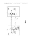
[0019]In a high-level block diagram, FIG. 1 depicts two circuit cards 10, 12, labeled respectively as printed circuit board (PCB) A and PCB B, that have been adapted to use improved timing compensation in accordance with an embodiment of the present invention. The two circuit cards 10, 12 communicate data in the form of PDUs over a bidirectional link 14 formed from two unidirectional serial links 16, 18. Data is transmitted from PCB A 10 to PCB B 12 over a first serial link 16 of the two serial links, and likewise data is transmitted from PCB B 12 to PCB A 10 over a second serial link 18 of the two serial links.
[0020]PCB A 10 includes a clock (CLK) module 20, a Transmitter (Tx) module 22, a receiver (Rx) module 24 and a clock recovery unit (CRU) 26. A control link 28 enables certain information as will be explained later to be conveyed from the receiver module 24 to the transmitter module 22. The clock recovery unit 26 recovers a clock signal from incoming data received over the second serial link 18 and provides a write clock to the receiver module 24 with which to write incoming data from the second serial link 18 into a receiver buffer (B) 30. The clock module 20 includes an oscillator (Osc) 32 that generates a signal frequency (F) falling within a given level of accuracy, e.g. 20 parts per million (ppm) or 50 ppm, from which the clock module 20 generates a transmit clock signal (Tx Clk). The transmit clock signal is used by the transmitter module 22 for timing of data sent on the first serial link 16 and is also used by the receiver module 24 for reading data from the receiver buffer 30.
[0021]PCB B 12 has the same functional elements with respect to the bidirectional link 14 as PCB A 10 and operates in the same manner regarding transmission and reception of data over the bidirectional link 14.
[0022]In order for each of the serial links 16, 18 to work properly, overflowing and underflowing the receiver buffer in the respective receiver module, e.g. receiver buffer 30 in receiver module 24, should be avoided. Overflows and underflows of the receiver buffers are possible because the clock modules of the respective circuit cards 10, 12 are not synchronized to each other. Therefore, the recovered clock signal from the clock recovery unit 26, which is recovered from incoming data received over the second serial link 18 and which is used to write data received from the same link into the receiver buffer 30, may have a slightly higher or slightly lower frequency than the transmit clock signal (Tx Clk) generated by the clock module 20, which is used for reading data from the receiver buffer 30. This difference in frequencies results in data being read from the receiver buffer 30 at a different rate than that at which new data is being written to the receiver buffer 30. Where the read data rate is higher than the write data rate an underflow condition will occur, and conversely when the read data rate is lower than the write data rate an overflow condition will occur. While it is desirable to avoid both conditions, an overflow condition is especially disadvantageous since it results in loss of data.
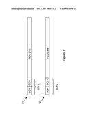
[0023]Since any typical serial link contains fixed PDUs of size 1 to n characters, a character being 8 bits in length, that periodically traverse the link, these datagrams consist of a special character sequence used solely to delineate the start of PDU (SOP). By extending and enhancing this special character sequence a multi-purpose function beyond its simple SOP definition can be achieved.
[0024]Referring to FIG. 2, two different SOP character sequences SOP1, SOP2 are used by the circuit cards 10, 12 shown in FIG. 1 to implement improved timing compensation in accordance with an embodiment of the present invention. A first PDU 34 starts with a first SOP character sequence SOP1 and a second PDU 36 starts with a second SOP character sequence SOP2. The first SOP character sequence SOP1 denotes that a near-end receiver buffer has a fill level that is within an acceptable range, e.g. is at or below a threshold which could be equal to a midpoint capacity of the receiver buffer. The term near-end is used with respect to a point of reference being one of either of the circuit cards 10, 12. For example, if the circuit card PCB A 10 is taken as the point of reference, near-end receiver buffer would mean the receiver buffer 30 of the circuit card PCB A 10. The second SOP character sequence SOP2 denotes that the near-end receiver buffer has a fill level that is outside the acceptable range, e.g. is above the threshold for the receiver buffer. The first SOP character sequence SOP1 comprises a first type of PDU delineator character (SCP) followed by another delineator character of the same type. The second SOP character sequence SOP2 comprises the first type of PDU delineator character (SCP) followed by a second type of PDU delineator character (SCP+). It should e noted that only one of the SOP characters sequences SOP1, SOP2 is included in a PDU.
[0025]Taking the circuit card PCB A 10 as the near-end point of reference, operation of the improved timing compensation in accordance with an embodiment of the present invention will now be explained. The receiver module 24 detects the fill level of its receiver buffer 30. Depending on whether the fill level is above or below a predetermined threshold, one of two respective control indications will be sent by the receiver module 24 to the transmitter module 22 over the control link 28. For example, if the fill level is at or below the threshold a first control indication will be sent, otherwise a second control indication will be sent. The transmitter module 22 receives the control indication and from that determines which SOP character sequence to append to the PDU data of the next PDU to be sent over the first serial link 16. If the transmitter module 22 receives the first control indication then it appends the first SOP character sequence SOP1 to the PDU data to form the next PDU that it will send. If the second control indication is received by the transmitter module 22 it will append the second SOP character sequence SOP2 to the PDU data to form the next PDU that it will send. The receiver module at the far-end circuit card PCB B 12 detects which of the two SOP character sequence was received with a given PDU and instructs the far-end transmitter module to adjust its transmission of data over the second serial link 18 accordingly. This adjustment will be explained below in reference to the circuit card PCB A 10.
[0026]Still taking the circuit card PCB A 10 as the near-end point of reference, when the receiver module 24 receives a PDU from the second serial link 18 it detects which of the two SOP character sequences was received with that PDU. If the first SOP character sequence SOP1 was received this denotes that the fill level of the far-end receiver buffer is within an acceptable range and no adjustment needs to be made to the transmission of data over the first serial link 16 by near-end transmitter module 22. However, if the second SOP character sequence SOP2 was received this denotes that the fill level of the far-end receiver buffer is outside an acceptable range and an adjustment is needed to the transmission of data over the first serial link 16 by the near-end transmitter module 22. In this case a third control indication is sent by the receiver module 24 to the transmitter module 22 over the control link 28. When the transmitter module 22 receives the third control indication delays the transmission of the next PDU by one character time, which is the duration of time required to transmit one character at the data rate of the first serial link 16. In this manner the far-end receiver module is given time to read one character from its receiver buffer before another character is written to the buffer, thereby reducing its buffer fill level. If necessary, the second SOP character sequence SOP2 can be included in multiple consecutive PDUs which will eventually bring the fill level of the far-end receiver buffer to within its acceptable range.
[0027]The use of the SOP character sequences, which are special character sequences, to uniquely define the start of a PDU as well as receiver buffer fill level at a near-end of a serial link enables a receiver module at the far-end of the serial link to uniquely identify these special character sequences as control information rather than simply data. This identification is made immediately upon reception of a given PDU rather than after forwarding to, and storing in, a buffering point as in the case of data characters. This immediate identification enables timely action to be taken at the far-end transmitter module to rectify any adverse fill level condition in the receiver buffer at the near-end of the serial link.
[0028]In the absence of PDU data to send on one of the serial links 16, 18 the respective transmitter module would periodically insert a unique PDU consisting of only an appropriate one of the SOP character sequences SOP1, SOP2 to signal the current status of the fill level of the near-end receiver buffer to the far-end receiver module. This enables far-end transmitter module to adjust its transmission of data to accommodate the fill level of the near-end receiver buffer even when there is no PDU data to be sent by the near-end transmitter module.
[0029]Numerous modifications and variations may be made to the embodiment of the invention described above without departing from the scope of the invention, which is defined in the claims. For example, a modification would be to use multiple receiver buffer thresholds to define a plurality of ranges of buffer fill levels, each of which range corresponding to a respective SOP character sequence that each in turn would cause a transmitter module to adjust its PDU transmission in a respective manner. For example, a second threshold could be defined corresponding to a 75% fill level of a receiver buffer and a corresponding third SOP character sequence SOP3 could be defined that causes a transmitter module to delay transmission of the next PDU by two character times. A variation would be to use only one character for each SOP character sequence. For example the first SOP character sequence SOP1 could comprise only the first type of PDU delineator character SCP, while the second SOP character sequence SOP2 could comprise only the second type of PDU delineator character SCP+. Another modification would be to eliminate the use of the first control indication and have the transmitter modules start each PDU with the first SOP character sequence SOP1 by default unless the second control indication is received, in which case the second SOP character sequence SOP2 would be appended to the next PDU data to be sent. Still another modification would be to combine the transmitter module 22 and receiver module 24 to form a single transceiver module having all the capabilities of the individual modules 22, 24 yet without the need for the control link 28 coupling the individual modules 22, 24.
[0030]It should now be apparent that the described embodiment, modifications, variations and adaptations of improved timing compensation on a bidirectional serial link provide advantages over existing timing compensation on such links. Specifically, the improved timing compensation more efficiently uses SOP characters by combining PDU delineation and buffer fill level information into those characters, which results in more efficient use of link bandwidth. Further to this point, the improvement alleviates the need for in-band insertion of timing compensation characters such as idle characters at fixed time intervals, thereby allowing more bandwidth for bearer data. Additionally, by eliminating in-band insertion of idle characters at fixed time intervals, design constraints on clock source accuracy are relaxed providing more design freedom, which advantageously offers the possibility of using inexpensive clock sources.
User Contributions:
comments("1"); ?> comment_form("1"); ?>Inventors list |
Agents list |
Assignees list |
List by place |
Classification tree browser |
Top 100 Inventors |
Top 100 Agents |
Top 100 Assignees |
Usenet FAQ Index |
Documents |
Other FAQs |
User Contributions:
Comment about this patent or add new information about this topic:
| People who visited this patent also read: | |
| Patent application number | Title |
|---|---|
| 20120298018 | PORTABLE SAFE, SYSTEMS AND METHODS |
| 20120298017 | DESK ASSEMBLY |
| 20120298016 | ADJUSTABLE TABLE COVERING |
| 20120298015 | PLASTIC PALLET STRUCTURE |
| 20120298014 | EXPANDABLE MODULAR INTERLOCKING PALLET SYSTEM |
Images included with this patent application:
 |  |
| New patent applications in this class: | |
| Date | Title |
|---|---|
| 2016-04-28 | Data transmitter apparatus and method for data communication using the same |
| 2016-03-17 | In-memory buffer service |
| 2016-02-04 | Input/output interceptor with intelligent flush control logic |
| 2015-01-15 | Semiconductor memory device having data compression test circuit |
| 2015-01-15 | Buffer memory reservation techniques for use with a nand flash memory |
| New patent applications from these inventors: | |
| Date | Title |
|---|---|
| 2009-12-31 | Providing backpressure flow control to specific traffic flows |
| 2009-04-02 | Method for communicating backpressure messages in a data communications system |
| 2009-03-26 | Egress traffic management system for a data communications system |
| Top Inventors for class "Electrical computers and digital data processing systems: input/output" | |
| Rank | Inventor's name |
|---|---|
| 1 | Daniel F. Casper |
| 2 | John R. Flanagan |
| 3 | Matthew J. Kalos |
| 4 | Mahesh Wagh |
| 5 | David J. Harriman |