Patent application title: Process for Measuring the Impedance of Electronic Circuits
Inventors:
Andrej Rumiantsev (Dresden, DE)
Stojan Kanev (Sacka, DE)
Assignees:
SUSS MicroTec Test Systems GmbH
IPC8 Class: AG01R2702FI
USPC Class:
702 65
Class name: Electrical signal parameter measurement system voltage or current including related electrical parameter
Publication date: 2008-11-13
Patent application number: 20080281537
Inventors list |
Agents list |
Assignees list |
List by place |
Classification tree browser |
Top 100 Inventors |
Top 100 Agents |
Top 100 Assignees |
Usenet FAQ Index |
Documents |
Other FAQs |
Patent application title: Process for Measuring the Impedance of Electronic Circuits
Inventors:
Andrej Rumiantsev
Stojan Kanev
Agents:
HESLIN ROTHENBERG FARLEY & MESITI PC
Assignees:
SUSS MICROTEC TEST SYSTEMS GMBH
Origin: ALBANY, NY US
IPC8 Class: AG01R2702FI
USPC Class:
702 65
Abstract:
The task underlying the invention, which concerns a method for measurement
of impedance of electronic circuits, in which the input of the electronic
circuit is acted upon by a high-frequency ac voltage with a measurement
frequency f as test signal and from the reaction of the circuit to the
test signal the impedance Z of the circuit is determined, in which a
parameter S, which represents the value
S = Z - Z 0 Z + Z 0
at a stipulated reference impedance Z0, is produced by means of an
analyzer with a reference impedance Z0, and from this parameter S
the impedance Z is determined, is to minimize the error in measuring the
impedances by determining parameter S. This is solved by the fact that
the measurement frequency f is set so that a minimal error ΔZ is
produced for Z.Claims:
1. Method for measurement of impedance of electronic circuits, in which
the input of the electronic circuit is acted upon by a high-frequency ac
voltage with a measurement frequency f as test signal and from the
reaction of the circuit to the test signal the impedance Z of the circuit
is determined, in which a parameter S, which represents the value S = Z
- Z 0 Z + Z 0 at a stipulated reference impedance Z0, is
produced by means of an analyzer with a reference impedance Z0 and
from this parameter S the impedance Z is determined with Z = Z 0
1 + S 1 - S ,characterized by the fact that the measurement
frequency f is set so that a minimal error ΔZ is obtained for Z
bydetermining a value Ze of the impedance of the circuit to be
expected with reference to the known characteristics of the
circuit,calculating with S e ( f ) = Z e ( f ) - Z 0
Z e ( f ) + Z 0 the expected value Se of the parameter
S,determining from the instrument-specific error curve ΔS=func(S)
known for the analyzer the corresponding error value
ΔSe=func(Se) for value Se,calculating from the
relation Δ Z e ( f ) = Z 0 1 + Δ
S e ( f ) 1 - Δ S e ( f ) for
different values of the measurement frequency f of the
frequency-dependent error value ΔZe(f) the impedance Ze
to be expected andsetting the measurement frequency f at a value at which
the error value ΔZe(f) of the impedance Ze to be expected
has a minimum.
2. Method according to claim 1, characterized by the fact that the impedance, which depends on the voltage V lying on it, is measured, characterized by the fact that, depending on voltage V, the measurement frequency f is set so that a minimal error ΔZ is obtained for Z bydetermining the expected value Ze(V) of the impedance in the circuit by means of the known characteristics of the circuit,calculating with S e ( V ; f ) = Z e ( V ; f ) - Z 0 Z e ( V ; f ) + Z 0 the values Se(V) to be expected for parameter S,determining from an instrument-specific error curve ΔS=func(S) known for the analyzer the error value ΔSe=func(Se) corresponding for a value Se,calculating from the relation Δ Z e ( f ; V ) = Z 0 1 + Δ S e ( f ; V ) 1 - Δ S e ( f ; V ) ,for different values of measurement frequency f and for different values of voltage V, the frequency-dependent error value ΔZe(f; V) of the expected impedance Ze and setting the measurement frequency f as a function of the voltage over the capacitance to a value at which the error value ΔZe(f; V) of the expected impedance Ze has a minimum.
3. Method according to claim 1 or 2, characterized by the fact that the impedance Ze to be expected is determined from an impedance substitution circuit of the circuit.
4. Method according to one of the claims 1 to 3, characterized by the fact that the impedance is formed essentially by a capacitance and the magnitude of the capacitance is determined by the impedance.
5. Method according to claim 4, characterized by the fact that the expected impedance is calculated with a stipulated calculation frequency fb and a calculated or simulated value Ce that is expected for capacitance C from Z e = - j 1 2 π f b C e .
6. Method according to one of the claims 1 to 5, characterized by the fact that determination of the setting of the measurement frequency is repeated and the frequency determined during the repeated run is used as measurement frequency, in which during repeated determination the impedance Z measured after the first measurement frequency determination is used as the expected value Ze during repetition of the determination.
Description:
[0001]The invention concerns a method for measurement of impedance of
electronic circuits in which the input of the electronic circuit is acted
upon with a high-frequency ac voltage with a measurement frequency f as
test signal and from the reaction of the circuit to the test signal the
impedance Z of the circuit is determined, in which a parameter S, which
represents the value
S = Z - Z 0 Z + Z 0
at a stipulated reference impedance Z0, is produced by means of an analyzer with a reference impedance Z0, and the impedance Z is determined from this parameter S with
Z = Z 0 1 + S 1 - S .
[0002]Both during the production process of electronic components and functional testing at the end of the production process it is often necessary to measure impedances of electronic circuits within an electronic component. A circuit arrangement being tested is ordinarily referred to as DUT (device under test).
[0003]Such impedances can be obtained as pure ohmic resistances R. Generally the impedances Z, however, are complex in nature, as expressed in the relation Z=R+jX, in which R is the real part (resistance) and X the imaginary part (reactance).
[0004]For example, the impedance of the circuit is determined by a capacitance C. If only capacitance has an effect on the impedance, then the real part equals zero. The impedance Z is then calculated as follows:
Z = - j 1 2 π fC .
[0005]Ordinarily capacitance measurement occurs by acting on the circuit or circuit input with a dc voltage or ac voltage up to 30 MHz. The magnitude of the capacitance can be determined by means of the time behavior of the measurement voltage.
[0006]The increasing miniaturization during production of electronic components has meant that dielectrics are becoming increasingly thinner. This means that the leakage currents through the dielectric are becoming larger. Such leakage currents have the drawback that they distort the measurement result for capacitance measurement. This is described in "Evaluation of MOS Capacitor Oxide C-V Characteristics Using the Agilent 4294A," Agilent Technologies, Inc., 2002, 5988-5102EN and especially page 29 there.
[0007]To counter this problem, impedances are increasingly being measured at higher frequencies in the range above 100 MHz. This means that the propagation region of the voltage in the capacitance is changed so that only the electromagnetic field still acts there and the leakage currents are minimized so that no electron loss occurs. The transmission and/or reflection factor is then measured (similarly to light). The ratio of transmitted and received wave magnitudes is then formed from the transmitted and received wave and produced as parameter S. This method is described in the presentation of different additional measurement methods in "Integrating high-frequency capacitance measurement for monitoring process variation of equivalent oxide thickness of ultrathin gate dielectrics," Keithley Instruments Inc., 2004, No. 24744041KGW. It is assumed that the measurement error on the reference impedance Z0 is minimal.
[0008]This type of measurement ordinarily occurs in a vector-network analyzer. These measurement instruments have a known error ΔS for parameter S. However, it has been shown that, contrary to the assumption in the prior art, the error minimum does not lie constantly at the same reference impedance. Instead, for a specific DUT this error ΔS is also dependent on the measurement frequency so that the measurement results obtained in this way are only marginally suitable.
[0009]Determination of ΔS ordinarily occurs with a method as described in EA-10/12-EA Guidelines on the Evaluation of Vector Network Analyzers (VNA), European Cooperation for Accreditation, May 2000 and in Application Note "What is your Measurement Accuracy? Vector Network Analyzer," Anritsu Microwave Measurement Division, Morgan Hill, Calif., September 2001.
[0010]The task of the invention now consists of minimizing the error during measurement of impedances by determining parameter S.
[0011]This task is solved according to the invention with the features of Claim 1. The dependent Claims 2 to 1 [sic] provide favorable embodiments of the method according to the invention.
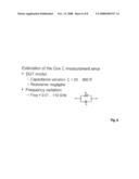
[0012]The invention is further described below by means of a practical example. This practical example pertains to capacitance measurement in MOSFET with thin gate oxides.
[0013]In the corresponding drawings
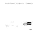
[0014]FIG. 1 shows a diagram of the measurement of the circuit with a vector network analyzer with determination of the capacitance C,
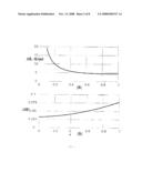
[0015]FIG. 2 shows the trend of the real and imaginary part of the error ΔS on the vector network analyzer (VNA),
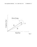
[0016]FIG. 3 shows a diagram of the appearance of the error ΔS,
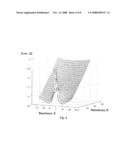
[0017]FIG. 4 shows a graph of the occurring error ΔZ of the impedance Z being measured in a complex plot,
[0018]FIG. 5 shows an excerpt from FIG. 4 relative to the imaginary part,
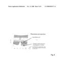
[0019]FIG. 6 shows a diagram of the replacement circuit of the impedance being measured and the parameter to be expected,
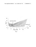
[0020]FIG. 7 shows a plot of the measurement frequency f to be chosen as a function of the capacitance to be expected and to achieve the least possible measurement error.
[0021]By means of a vector network analyzer (VNA) an impedance ZDUT of an electronic circuit (not further shown) within an electronic component (DUT=device under test) is determined via parameter S, as shown in FIG. 1. The actual parameters of the DUT are ZDUT=R+jX and
S DUT = R + j X - Z 0 R + j X + Z 0 .
The measured impedance value is
Z meas = Z 0 1 + S meas 1 - S meas .
[0022]As shown in FIG. 2, the vector network analyzer (VNA) has an error ΔS that also causes an error in the impedance ΔZ being measured. Because of the error ΔS, Smeas=SDUT+ΔS is obtained and therefore
Z meas = Z 0 1 + ( S DUT + Δ S ) 1 - ( S DUT + Δ S ) .
The error for the impedance
Δ Z = Z DUT - Z meas Z DUT
follows from this.
[0023]FIG. 3 shows the effects of complexity of the error ΔS on the measurement result.
[0024]It is found that the impedance ZDUT being measured is dependent on the measurement frequency. The parameter S of the circuit being measured is also dependent on the impedance ZDUT being measured. Consequently, the measurement accuracy of the vector network analyzer depends on parameter S.
[0025]As shown in FIGS. 4 to 6, an estimate of error ΔS occurs according to the invention at different frequencies.
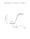
[0026]As is apparent from FIG. 7, the measurement frequency f should be chosen relative to the expected capacitances C from the marked area of the diagram in order to be able to determine the capacitance as precisely as possible.
[0027]As shown in FIG. 8, it is also possible with the method according to the invention to state the error range (error bars) in which the achieved measurement result fluctuates.
User Contributions:
comments("1"); ?> comment_form("1"); ?>Inventors list |
Agents list |
Assignees list |
List by place |
Classification tree browser |
Top 100 Inventors |
Top 100 Agents |
Top 100 Assignees |
Usenet FAQ Index |
Documents |
Other FAQs |
User Contributions:
Comment about this patent or add new information about this topic:
Images included with this patent application:
 |  |
 |  |
 |  |
 |  |
 |  |
 |
| Similar patent applications: | |
| Date | Title |
|---|---|
| 2012-01-19 | System and method for measuring performance of electronic products |
| 2008-09-25 | Acquiring test data from an electronic circuit |
| 2012-12-13 | Process for estimation of ballistic missile boost state |
| 2009-12-24 | Device for measuring the purity of ultrapure water |
| 2010-02-18 | Methods for measurement of fluid electrical stability |
| New patent applications from these inventors: | |
| Date | Title |
|---|---|
| 2011-12-01 | Chuck for supporting and retaining a test substrate and a calibration substrate |
| 2011-09-22 | Probe station for on-wafer-measurement under emi-shielding |
| 2010-11-25 | Probe holder |
| 2010-11-18 | Method for testing a test substrate under defined thermal conditions and thermally conditionable prober |
| 2010-04-29 | Process for measuring the impedance of electronic circuits |
| Top Inventors for class "Data processing: measuring, calibrating, or testing" | |
| Rank | Inventor's name |
|---|---|
| 1 | Lowell L. Wood, Jr. |
| 2 | Roderick A. Hyde |
| 3 | Shelten Gee Jao Yuen |
| 4 | James Park |
| 5 | Chih-Kuang Chang |