Patent application title: PRINTED WIRING BOARD
Inventors:
Nobuhisa Sugimoto (Yamanashi, JP)
Takeshi Sawada (Yamanashi, JP)
IPC8 Class: AH05K111FI
USPC Class:
Class name:
Publication date: 2015-08-27
Patent application number: 20150245482
Abstract:
In a printed wiring board on which an electronic component comprising
electrode terminal rows on four peripheral sides or two opposite sides
thereof is mounted, each of pads at the both ends of pad rows
corresponding to the electrode terminal rows extend outwardly relative to
the other pads in the direction of arrangement of the pads and has a
shape obtained by diagonally cutting a corner located farthest from the
center of the electronic component.Claims:
1. A printed wiring board on which an electronic component comprising
electrode terminal rows on four peripheral sides or two opposite sides
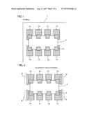
thereof is mounted, the printed wiring board comprising: pad rows
corresponding to the electrode terminal rows; and each of pads at the
both ends of the pad rows comprises an extension extending outwardly
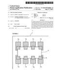
relative to the other pads in the direction of arrangement of the pads
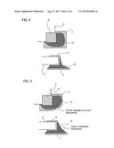
from the center of the electronic component, the extension having a shape
obtained by diagonally cutting a corner located farthest from the center
of the electronic component.
2. The printed wiring board according to claim 1, wherein each of the pads at the both ends has a shape obtained by diagonally cutting the end pad by a segment which connects the points of intersection of two sides between which the corner of the electronic component is located and perpendicular lines extending from the corner to the two sides.
3. The printed wiring board according to claim 1, wherein each of the pads at the both ends comprises an extension extending outwardly in a direction perpendicular to the direction of arrangement of the pads, as well as in the direction of arrangement of the pads, from the center of the electronic component.
Description:
BACKGROUND OF THE INVENTION
[0001] 1. Field of the Invention
[0002] The present invention relates to a printed wiring board on which electronic components are mounted.
[0003] 2. Description of the Related Art
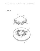
[0004] Conventionally, an electronic component 3 is mounted on pads 7 of a printed wiring board 1 in the following manner. As shown in FIG. 6, the rectangular pads 7 are arranged on the printed wiring board 1, depending on the shape, size, layout, etc., of electrode terminals 5 of the electronic component 3. A solder paste is applied to the pads 7 and the electronic component 3 is placed on the paste. The entire structure is heated by a reflow device. The electronic component 3 is mounted on the pads 7 as the solder paste is melted so that the electrode terminals 5 of the electronic component 3 are soldered to the pads 7 of the printed wiring board 1. In FIG. 6, numerals 2, 4 and 6 designate a mounting area, the body, and wiring, respectively. Japanese Patent Application Laid-Open No. 7-183650 relates to this technique.
[0005] The conventional technique shown in FIG. 6 has a problem that a large stress is applied to soldered portions of those pads 7 which are located at the both ends of pad rows during a temperature cycle so that surrounding elements are liable to fail due to rupture of the soldered portions.
SUMMARY OF THE INVENTION
[0006] Accordingly, the object of the present invention is to provide a printed wiring board configured so that the rupture life of soldered portions of pads thereon can be extended.
[0007] According to the present invention, each of pads at the both ends of pad rows that are most heavily stressed during a temperature cycle comprises an extension extending outwardly in the direction of arrangement of the pads from the center of an electronic component, the extension having a shape obtained by diagonally cutting a corner of the pad located farthest from the center of the electronic component.
[0008] A printed wiring board according to the present invention is mounted with an electronic component comprising electrode terminal rows on four peripheral sides or two opposite sides thereof. The printed wiring board comprises pad rows corresponding to the electrode terminal rows and each of pads at the both ends of the pad rows comprises an extension extending outwardly relative to the other pads in the direction of arrangement of the pads from the center of the electronic component, the extension having a shape obtained by diagonally cutting a corner located farthest from the center of the electronic component.
[0009] Each of the pads at the both ends may have a shape obtained by diagonally cutting the end pad by a segment which connects the points of intersection of two sides between which the corner farthest from the center of the electronic component is located and perpendicular lines extending from the corner to the two sides.
[0010] Each of the pads at the both ends may comprise an extension extending outwardly in a direction perpendicular to the direction of arrangement of the pads, as well as in the direction of arrangement of the pads, from the center of the electronic component.
[0011] According to the present invention configured as described above, there can be provided a printed wiring board configured so that the rupture life of soldered portions of pads thereon can be extended.
BRIEF DESCRIPTION OF THE DRAWINGS
[0012] The above and other objects and features of the present invention will be obvious from the ensuing description of embodiments with reference to the accompanying drawings, in which:
[0013] FIG. 1 is a view showing how an electronic component is placed on pads of a printed wiring board;
[0014] FIG. 2 is a view showing how outermost pads of FIG. 1 are extended;
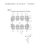
[0015] FIG. 3 is a view showing how the outermost pads of FIG. 2 are extended and their corners are cut;
[0016] FIG. 4 is a view showing how an outermost pad and an electrode terminal of FIG. 2 are soldered to each other;
[0017] FIG. 5 is a view showing how an outermost pad and an electrode terminal of FIG. 3 are soldered to each other; and
[0018] FIG. 6 is a view showing a conventional technique.
DETAILED DESCRIPTION OF THE PREFERRED EMBODIMENTS
[0019] FIG. 1 is a view showing how an electronic component is placed on pads of a printed wiring board. In the present embodiment, each pad is rectangular. A printed wiring board 1 is provided with pads 7 on which an electronic component 3 is mounted. The electronic component 3 is, for example, an electronic component provided with a plurality of electrode terminals 5. Four electrode terminals 5 are arranged side by side on each of two opposite sides of the electronic component 3. In the present embodiment, the electrode terminals 5 are arrayed on four peripheral sides or two opposite sides of the electronic component 3. The electrode terminals 5 of the electronic component 3 and the pads 7 on the printed wiring board 1 are electrically connected and secured to one another by soldering.
[0020] FIG. 2 is a view showing how the outermost pads of FIG. 1 are extended. The four outermost ones of the pads (7a, 7b, 7c, 7d, 7e, 7f, 7g and 7h) are designated by 7a, 7d, 7e and 7h, individually. The outermost pads 7a, 7d, 7e and 7h are located individually at the both ends of pad rows corresponding to the rows of the electrode terminals 5 of the electronic component 3.
[0021] These pads 7a, 7d, 7e and 7h are extended outwardly relative to the other pads in the direction of their arrangement. Thus, each of the outermost pads has an extension (designated by numeral 8 in FIG. 2), which extends outwardly in the direction of arrangement of the pads from the center of the electronic component.
[0022] FIG. 3 is a view showing how the outermost pads of FIG. 2 are extended and their corners are cut. "Cutting" here denotes partially removing the pads. Each of the outermost pads 7a, 7d, 7e and 7h has a shape obtained by diagonally cutting a corner or apex portion (see FIG. 2) located farthest from a center 9 of the electronic component 3. Numeral 10 designates a cut portion. A cut line 11 of each of the pads 7a, 7d, 7e and 7h at the both ends is a segment that connects the points of intersection of two sides between which a corner of the electronic component is located and perpendicular lines extending from the corner to the two sides. Further, each of the outermost pads 7a, 7d, 7e and 7h may be extended outwardly in a direction 13 perpendicular to a direction 12 of arrangement of the pads, as well as in the direction 12.
[0023] FIG. 4 is a view showing how an outermost pad and an electrode terminal of FIG. 2 are soldered to each other. In FIG. 4, numeral 14 designates a solder fillet. FIG. 5 is a view showing how an outermost pad and an electrode terminal of FIG. 3 are soldered to each other. A larger solder fillet can be formed to improve the resistance to temperature cycling by outwardly extending the pad 7 and increasing the solder supply. As shown in FIG. 5, moreover, the solder fillet can be increased in thickness to also improve the temperature cycling resistance by cutting a corner to prevent extra trailing of the solder fillet.
User Contributions:
Comment about this patent or add new information about this topic:
Images included with this patent application:
 |  |
 |  |
 |
| New patent applications in this class: | |
| Date | Title |
|---|---|
| 2022-09-08 | Shrub rose plant named 'vlr003' |
| 2022-08-25 | Cherry tree named 'v84031' |
| 2022-08-25 | Miniature rose plant named 'poulty026' |
| 2022-08-25 | Information processing system and information processing method |
| 2022-08-25 | Data reassembly method and apparatus |
| New patent applications from these inventors: | |
| Date | Title |
|---|---|
| 2015-11-05 | Printed circuit board and method of manufacturing the same |