Patent application title: GUIDED PATH FOR FORMING A CONDUCTIVE FILAMENT IN RRAM
Inventors:
Sung Hyun Jo (Sunnyvale, CA, US)
Sung Hyun Jo (Sunnyvale, CA, US)
IPC8 Class: AH01L4500FI
USPC Class:
Class name:
Publication date: 2015-06-04
Patent application number: 20150155480
Abstract:
A method of forming a non-volatile memory device, includes forming a
first electrode above a substrate, forming a dielectric layer overlying
the first electrode, forming an opening structure in a portion of the
dielectric layer to expose a surface of the first electrode having an
aspect ratio, forming a resistive switching material overlying the
dielectric layer and filling at least a portion of the opening structure
using a deposition process, the resistive switching material having a
surface region characterized by a planar region and an indent structure,
the indent structure overlying the first electrode, maintaining a first
thickness of resistive switching material between the planar region and
the first electrode, maintaining a second thickness of resistive
switching material between the indent structure and the first electrode,
wherein the first thickness is larger than the second thickness, and
forming a second electrode overlying the resistive switching material
including the indent structure.Claims:
1. A resistive switching device for a non-volatile memory device,
comprising: a first electrode; a resistive switching material configured
in an opening region in a dielectric material overlying the first
electrode, the resistive switching material being characterized by a
surface region having a planar region and an indent structure, at least a
portion of the planar region being configured overlying the first
electrode while maintaining a first thickness of resistive switching
material relative to the first electrode, the indent structure being
configured overlying the first electrode while maintaining a second
thickness of resistive switching material relative to the first
electrode, wherein the first thickness exceeds the second thickness; and
a second electrode overlying the resistive switching material including
the indent structure.
2. The device of claim 1 wherein the first electrode comprises a p+ polysilicon material.
3. The device of claim 1 wherein the resistive switching material comprises an amorphous silicon material having an intrinsic semiconductor characteristic, wherein the amorphous silicon material is not intentionally doped.
4. The device of claim 1 wherein second electrode comprises an active metal material selected from a group consisting of: silver, gold, palladium, platinum, copper, aluminum, nickel, and zinc.
5. The device of claim 1 wherein the indent structure comprises a tapered region directed towards the first electrode.
6. The device of claim 1 wherein the indent structure is configured to cause a path for a filament structure derived from the second electrode to preferentially form within the region of the indent structure within the resistive switching material upon application of a positive voltage to the second electrode with respect to the first electrode.
7. The device of claim 1 wherein the filament structure causes the resistive switching material to change from a high resistance state to a low resistance state upon application of the positive voltage to the second electrode.
8. The device of claim 6 wherein the resistive switching material comprises metal material from the second electrode disposed within the path.
9. The device of claim 1 wherein the first electrode comprises a material selected from a group consisting of Ti, TiN, WN, TaN.
10. The device of claim 1 wherein the resistive switching material is not intentionally doped as deposited and comprises a plurality of defect sites; and wherein metal particles from the second electrode diffuse into defect sites in the resistive switching material.
11. A device having a non-volatile memory device, comprising: a first dielectric material disposed adjacent to a substrate and having a first surface; a first electrode comprising first electrode material disposed adjacent to a first portion of the first surface of first dielectric material and having a first surface; a second dielectric material adjacent to a second portion of the first surface of the first electrode material and having a first surface; a resistive switching material adjacent to and in contact with at least a portion of the first surface of the first electrode material and at least a portion of the first surface of the second dielectric material, wherein the resistive switching material having a first surface, and wherein the resistive switching material comprises a plurality of defects and as-deposited is not intentionally doped; and a second electrode comprising a second electrode material disposed adjacent to and in contact with the first surface of the resistive switching material, wherein the second electrode material comprises a plurality of metal particles that are configured to be diffused within the resistive switching material upon application of a bias voltage; and wherein metal particles from the plurality of metal particles are disposed within the plurality of defects in the resistive switching material.
12. The device of claim 11 wherein the first surface of the resistive switching material comprises a portion disposed above the portion of the first surface of the first electrode material and includes an indent structure, and wherein an average thickness of the resistive switching material within the portion is larger than a thickness of the resistive switching material within the indent structure.
13. The device of claim 11 further comprising a control circuitry disposed on the substrate, wherein the control circuitry is coupled to the first electrode.
14. The device of claim 13 wherein the control circuitry is selected from a group consisting of: write circuitry, read circuitry, erase circuitry.
15. The device of claim 11 wherein the first electrode comprises a material selected from a group consisting of Ti, TiN, WN, TaN.
16. The device of claim 15 wherein second electrode material comprises an active metal material selected from a group consisting of: gold, palladium, platinum, copper, aluminum, and nickel.
17. The device of claim 11 wherein the resistive switching material is selected from a group consisting of: an undoped silicon-bearing material, an intrinsic semiconductor material.
18. The device of claim 11 wherein the metal particles from the plurality of metal particles from the first electrode are disposed along a predetermined path within the resistive switching material.
19. The device of claim 11 wherein a resistance associated with the resistive switching material as-deposited is different from a resistance associated with the resistive switching material having the metal particles disposed therein.
20. The device of claim 11 wherein the metal particles disposed within the resistive switching material form a filament structure extending from the second electrode towards the first electrode.
Description:
REFERENCE TO RELATED APPLICATIONS
[0001] This application is a divisional of and claims priority to U.S. patent application Ser. No. 13/462,653, filed May 2, 2012, which is related to U.S. patent application Ser. 13/156,232 filed Jun. 8, 2011, which claims priority to U.S. Provisional Application No. 61/352, 761 filed Jun. 8, 2010, commonly assigned, and incorporated herein by reference for all purpose.
BACKGROUND
[0002] The present invention is related to switching devices. More particularly, the present invention provides a device structure and a method to form a resistive switching device having an improved switching performance. Embodiments of the present invention have been applied to a non-volatile memory device. But it should be recognized that the present invention can have a much broader range of applicability.
[0003] The inventor of the present invention has recognized the success of semiconductor devices has been mainly driven by an intensive transistor down-scaling process. However, as field effect transistors (FETs) approach sizes less than 100 nm, physical problems such as short channel effect begin to hinder proper device operation. For transistor based memories, such as those commonly known as Flash memories, other performance degradations or problems may occur as device sizes shrink. With Flash memories, a high voltage is usually required for programming of such memories, however, as device sizes shrink, the high programming voltage can result in dielectric breakdown and other problems. Similar problems can occur with other types of non-volatile memory devices other than Flash memories.
[0004] The inventor of the present invention recognizes that many other types of non-volatile random access memory (RAM) devices have been explored as next generation memory devices, such as: ferroelectric RAM (Fe RAM); magneto-resistive RAM (MRAM); organic RAM (ORAM); phase change RAM (PCRAM); and others.
[0005] A common drawback with these memory devices include that they often require new materials that are incompatible with typical CMOS manufacturing. As an example of this, Organic RAM or ORAM requires organic chemicals that are currently incompatible with large volume silicon-based fabrication techniques and foundries. As another example of this, Fe-RAM and MRAM devices typically require materials using a high temperature anneal step, and thus such devices cannot be normally be incorporated with large volume silicon-based fabrication techniques.
[0006] Additional drawbacks with these devices include that such memory cells often lack one or more key attributes required of non-volatile memories. As an example of this, Fe-RAM and MRAM devices typically have fast switching (e.g. "0" to "1") characteristics and good programming endurance, however, such memory cells are difficult to scale to small sizes. In another example of this, for ORAM devices reliability of such memories is often poor. As yet another example of this, switching of PCRAM devices typically includes Joules heating and undesirably require high power consumption.
[0007] From the above, improved semiconductor memory devices that can scale to smaller dimensions with reduced drawbacks are therefore desirable.
BRIEF SUMMARY OF THE PRESENT INVENTION
[0008] The present invention is related to switching devices. More particularly, the present invention provides a device structure and a method to form a resistive switching device having an improved switching performance. Embodiments of the present invention have been applied to a non-volatile memory device. But it should be recognized that the present invention can have a much broader range of applicability.
[0009] According to one aspect of the invention, a method of forming a resistive switching device for a non-volatile memory device is disclosed. One technique includes providing a substrate having a surface region, forming a first dielectric material overlying the surface region of the substrate, and forming a first electrode structure in a portion of the first dielectric material. A process includes forming a second dielectric material overlying the first electrode, forming an opening structure in a portion of the second dielectric material to expose a surface region of the first electrode structure, the opening structure being characterized by an aspect ratio, and forming a resistive switching material overlying the second dielectric material and filling at least a portion of the opening structure using a deposition process, the resistive switching material having a surface region characterized by a planar region and an indent structure, the indent structure overlying the first electrode structure. A method includes maintaining a first thickness of resistive switching material between the planar region and the first electrode structure, maintaining a second thickness of resistive switching material between the indent structure and the first electrode structure, wherein the first thickness is larger than the second thickness, and forming a second electrode structure overlying the resistive switching material including the indent structure.
[0010] According to another aspect of the invention, a resistive switching device for a non-volatile memory device is disclosed. A device may include a first electrode, and a resistive switching material configured in an opening region in a dielectric material overlying the first electrode, the resistive switching material being characterized by a surface region having a planar region and an indent structure, at least a portion of the planar region being configured overlying the first electrode while maintaining a first thickness of resistive switching material relative to the first electrode, the indent structure being configured overlying the first electrode while maintaining a second thickness of resistive switching material relative to the first electrode, wherein the first thickness exceeds the second thickness. An apparatus may include a second electrode overlying the resistive switching material including the indent structure.
[0011] According to yet another aspect of the invention, a resistive switching device is formed according to a method. One technique includes providing a substrate having a surface region, forming a first dielectric material overlying the surface region of the substrate, and forming a first electrode in a portion of the first dielectric material. A process includes forming a second dielectric material overlying the first electrode, forming an opening structure in a portion of the second dielectric material to expose a surface region of the first electrode structure, the opening structure being characterized by an aspect ratio, and forming a resistive switching material overlying the second dielectric material and filling at least a portion of the opening structure using a deposition process, the resistive switching material having a surface region characterized by a planar region and an indent structure, the indent structure overlying the first electrode structure. A method may include maintaining a first thickness of resistive switching material between the planar region and the first electrode structure, maintaining a second thickness of resistive switching material between the indent structure and the first electrode structure, wherein the first thickness is larger than the second thickness, and forming a second electrode structure overlying the resistive switching material including the indent structure.
[0012] In a specific embodiment, a method of forming a resistive switching device for a non-volatile memory device is provided. The method includes providing a substrate having a surface region and forming a first dielectric material overlying the surface region of the substrate. The method includes forming a first electrode structure overlying the first dielectric material and forming a resistive switching material structure overlying the first electrode. The resistive switching material structure includes a vertical side wall region. In various embodiment, the method forms a second dielectric material overlying the resistive switching material structure including the side wall region and forms a first material derived from the resistive switching material and the second dielectric material in a first material region in a vicinity of the side wall region. A second electrode structure is formed overlying the resistive switching material structure including the first material region.
[0013] In a specific embodiment, a resistive switching device for a non-volatile memory device is provided. The device includes a first electrode structure, a resistive switching material structure overlying the first electrode. The resistive switching material structure includes a resistive switching material having a vertical side wall region. A dielectric material overlies the resistive switching material structure including the vertical side wall region. The device includes a first material region comprising a first material configured in a vicinity of the vertical side wall region. In various embodiments, the first material is formed and derived from the dielectric material and the resistive switching material. A second electrode is configured overlying the resistive switching material structure and the first material region. In various embodiments, the first material region provides a path and facilitates formation of a conductive structure derived from the second electrode upon application of a programming voltage.
[0014] Many benefits can be achieved by ways of the present invention over conventional techniques. For example, embodiments according to the present invention provide various methods and device structures to form a conductive filament structure in a resistive switching device to change a resistance state or bit value of the device. The device is characterized by a low operating voltage (for example, low programming voltage) and a well defined region to form the conductive filament structure for a robust fabrication method. Additionally, various devices according to the present invention can be characterized by a good endurance, reliable and fast switching among others. Additionally, the present device can have programmed to more than one resistive state for a multibit device. The present device disposed in a crossbar configuration can be vertically integrated to form a high density memory device thus drastically reduce cost per bit, a major attribute for present and future application in consumer devices. The present device can be implemented in a vast variety of applications such as date storage, code storage, embedded devices, for example, as configuration bit for field programmable gate array, radiation hardened application, and others. The present device can be configured to be write once read many times, write many times read once, or fully re-writable. Depending on the application, one or more of these benefits can be achieved.
SUMMARY OF THE DRAWINGS
[0015] In order to more fully understand the present invention, reference is made to the accompanying drawings. Understanding that these drawings are not to be considered limitations in the scope of the invention, the presently described embodiments and the presently understood best mode of the invention are described with additional detail through use of the accompanying drawings in which:
[0016] FIGS. 1 and 2 are simplified diagram illustrating a conventional resistive switching device and its operation;
[0017] FIGS. 3-13 are simplified diagrams illustrating a method of forming a resistive switching device for a non-volatile memory device according to various embodiments of the present invention;
[0018] FIGS. 14-21 are simplified diagrams illustrating an alternative method of forming a resistive switching device for a non-volatile memory device according to various embodiments of the present invention; and
[0019] FIG. 22 is a scanning electron microscope image of an amorphous silicon material surface structure formed according to various embodiment of the present invention.
DETAILED DESCRIPTION OF THE PRESENT INVENTION
[0020] The present invention is related to switching devices. More particularly, the present invention provides a device structure and a method to form a resistive switching device having an improved switching performance. Embodiments of the present invention have been applied to a non-volatile memory device. But it should be recognized that the present invention can have a much broader range of applicability.
[0021] The growth of consumer devices has led to an ever increasing demand for high density memory storage at a low cost per bit. Data storage of current non-volatile memory devices are based on charges stored in a floating gate or a dielectric layer. Scaling of these devices is limited as these devices usually require a transistor device coupled to a memory cell. Further down scale of transistors may not be possible due to short channel effects and others. Additionally, as these devices are three terminal devices, vertical or three dimensional integration of memory cells are difficult to achieve. Switching devices for memory cells arranged in a crossbar configuration can provide a method and a structure for high density integration at a much reduced cost.
[0022] Resistive switching device is a two terminal device having a resistive switching material configured in an intersection region of a first electrode and a second electrode. For resistive switching devices using amorphous silicon material as a switching material, the switching mechanism or state change mechanism can be based on a filament structure derived from a conductive material formed in the amorphous silicon material upon application of an electric field. The conductive material can be derived from, for example, the second electrode. The formation of the conductive structure and its interaction with the amorphous silicon material as well as its interaction with the first electrode would affect the switching characteristic thus the performance of the device. As the filament structure is formed in grain boundaries of the amorphous silicon material, switching voltage is usually quite low (no greater than about 6 or 7 volts). However, grain structures in amorphous silicon material are random; the filament structure might have variations from device to device affecting device yield and performance. Embodiments according to the present provide a method and a device structure for a well defined path or preferred path for the formation of the filament structure.
[0023] FIG. 1 is a simplified diagram illustrating a conventional switching device structure 100. As shown, the convention switching device includes a first electrode 102, a second electrode 104, and a switching material 106 sandwiched between first electrode 102 and second electrode 104. Second electrode 104 can have a portion that includes a metal material. For switching material 106 using an amorphous silicon material, the metal material can be silver, platinum, palladium, or other suitable metal materials having a suitable diffusivity characteristic in the amorphous silicon material. As shown, upon application of a first voltage 112, a metal region 108 is formed in switching material 106 and in contact with the top electrode. The metal region is formed largely by a diffusion mechanism, assisted by an electric field resulting from the first voltage 112.
[0024] FIG. 2 illustrates growth of metal region 108 in switching material 106 for the conventional resistive switching device. The diffusion of the metal material from second electrode 104 into the switching material is assisted by first voltage 112 and sometimes results in a continuous metal region. As metal region 108 grows, an end region of metal region 108 becomes sharper and closer to the bottom electrode. Once the end region is sharp enough and close enough to the bottom electrode, the electric field would have a much greater effect on the metal region growth than diffusion. As in FIG. 2, a filament structure 202 is formed by hopping of a metal particle from a defect site to the next defect site in the amorphous silicon material upon application of a suitable voltage. Therefore formation of filament structure 202 is due to the presence of the electric filed and aided by diffusion in contrast to the metal region growth. Metal region 108 including filament structure 202 form a conductive path for the resistive switching device. As diffusion of material can be uncontrollable, it is desirable that the formation of metal region especially filament structure 202 can be in a predetermined path controlled substantially by applied electric field.
[0025] FIGS. 3-13 illustrate a method for forming a resistive switching device according to various embodiments of the present invention. As shown in FIG. 3, a substrate 302 having a surface region 304 is provided. The substrate can be a semiconductor material such as monocrystalline silicon, silicon on insulator (SOI), silicon germanium, and polycrystalline silicon, and others. Depending on the embodiments, the substrate can further include one or more transistor device formed thereon. The one or more transistor device can be controlling circuitry for the resistive switching device.
[0026] In certain embodiments, the semiconductor substrate 302 can have one or more MOS devices formed thereon. The one or more MOS devices can be controlling circuitry for the resistive memory devices in specific embodiments. In other embodiments, the one or more MOS devices may include other functionality, such as a processor, logic, or the like.
[0027] In various embodiments, a processor, or the like, may include resistive memory memories as described herein. Because the state-change memories are relatively non-volatile, the states of devices, such as processors, or the like may be maintained while power is not supplied to the processors. To a user, such capability would greatly enhance the power-on power-off performance of devices including such processors. Additionally, such capability would greatly reduce the power consumption of devices including such processors. In particular, because such memories are non-volatile, the processor need not draw power to refresh the memory states, as is common with CMOS type memories. Accordingly, embodiments of the present invention are directed towards processors or other logic incorporating these memory devices, as described herein, devices (e.g. smart phones, network devices) incorporating such memory devices, and the like.
[0028] Referring to FIG. 4, the method includes forming a first dielectric material 402 overlying surface region 304 of substrate 302. First dielectric material 402 can be silicon oxide, silicon nitride, silicon oxynitride, a high K dielectric, a low K dielectric, or a dielectric stack having alternating layer of silicon oxide and silicon nitride (for example an ONO stack), including any combination of these, and others. First dielectric material 402 can be deposited using techniques such as chemical vapor deposition, including low pressure chemical vapor deposition, plasma enhanced chemical vapor deposition, high density plasma chemical vapor deposition, atomic layer deposition (ALD), physical vapor deposition, spin on coating, including any combination of these, and others.
[0029] As shown in FIG. 5, the method includes forming a first electrode material 502 overlying first dielectric material 402. First electrode material 502 can be a suitable metal material including alloy materials, or a semiconductor material having a suitable conductivity characteristic. The metal material can be tungsten, aluminum, copper or silver, and others.
[0030] These metal materials may be deposited using a physical vapor deposition process, chemical vapor deposition process, electroplating, or electroless deposition process, including any combinations of these, and others. The semiconductor material can be, for example, a suitably doped silicon material in certain embodiments. In certain embodiments, first electrode material 502 can include one or more adhesion material or diffusion material to prevent the metal material to contaminate portions of the device in certain embodiments. Diffusion barrier material or adhesion material may each include titanium, titanium nitride, tungsten nitride, tantalum nitride, and others. The semiconductor material can be a doped polysilicon material depending on the implementation.
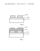
[0031] Referring to FIG. 6, the method subjects first electrode material 502 to a first pattern and etch process to form a plurality of first electrode structure(s) 602 overlying first dielectric material 402. For a crossbar configuration, first electrode structure 602 is spatially configured to extend in a first direction (e.g. in and out of the page).
[0032] As shown in FIG. 7, a second dielectric material 702 is deposited overlying the plurality of first electrode structure 602 to isolate each of the plurality of first electrode structure 602.
[0033] Second dielectric material 702 can include silicon oxide, silicon nitride, silicon oxynitride, a high K dielectric, a low K dielectric, or a dielectric stack having alternating layer of silicon oxide and silicon nitride (for example an ONO stack), including any combination of these, and others. Second dielectric material 702 can be deposited using techniques such as chemical vapor deposition, including low pressure chemical vapor deposition, plasma enhanced chemical vapor deposition, high density plasma chemical vapor deposition, atomic layer deposition (ALD), physical vapor deposition, spin on coating, including any combination of these, and others.
[0034] Referring to FIG. 8. Second dielectric material 702 is subjected to a planarizing process to form a substantially planarized surface region 802 and maintaining a thickness 804 of second dielectric material 702 overlying first electrode structure(s) 602. The planarizing process can be a chemical/mechanical process, an etch back process, a combination thereof, and others. Alternatively, the planarizing process can remove a portion of second dielectric material 702 to expose a surface region of first electrode structure 602 and a thickness 804 of second dielectric material can then be deposited overlying the exposed surface region of the first electrode structure 602.
[0035] As shown in FIG. 9, in various embodiments, an opening structure 902 is formed in portions of the second dielectric material 702 to expose a surface region 904 of first electrode structure 602. First opening structure can be a trench structure configured substantially parallel to the first direction of the first electrode stricture(s) 602 in various embodiments. Opening structure 902 is characterized by an aspect ratio (ratio of height (up and down on the page) to width (left and right on the page).
[0036] Referring to FIG. 10, the method includes forming a resistive switching material 1002 overlying the second dielectric material and to fill opening structure 902. Resistive switching material can be a non-conductive material characterized by an electric resistance depending on an electric field present in the resistive switching material. In various embodiments, the resistive switching material can be an amorphous silicon material having an intrinsic semiconductor characteristic or intrinsic amorphous silicon material. The intrinsic semiconductor characteristic is maintained by not intentionally doping the amorphous silicon material during deposition or after deposition.
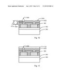
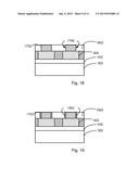
[0037] The intrinsic amorphous silicon material 1002 may be deposited using a conformal deposition process to form a surface region 1004 having a planar region and an indent structure 1006. The conformal deposition can be a chemical vapor deposition process that provides a good step coverage for the resistive switching material. The indent structure is characterized by a width and a depth that can be determined by the deposition process parameters (for example, deposition rate, deposition temperature, and others) as well as the aspect ratio of the opening structure 902. As shown, indent structure 1006 has a tapered structure directed towards first electrode structure 602 and a thickness 1008 of resistive switching material 1002 is maintained between indent structure 1006 and first electrode structure 602. As can be seen in the figure, thickness 1008 is thinner than a thickness 1010 between the planar region of surface region 1004 and first electrode structure 602.
[0038] In various embodiments, because thickness 1008 is thinner than thickness 1010, when an electric field is applied across the resistive switching material 1002, a metallic filament, as described herein is preferentially formed within the region of indent structure 1006.
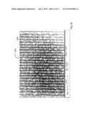
[0039] A scanning electron microscope image 2200 of an amorphous silicon material surface is illustrated in FIG. 22. The amorphous silicon material is formed by steps as illustrated in FIGS. 3-10. Dark regions as reference by numeral 2202 are the indent structures.
[0040] Referring to FIG. 11, the method includes forming a second electrode material 1102 overlying resistive switching material 1002 filling indent structure 1006, as shown. For amorphous silicon material as the resistive switching material, second electrode material 1102 may be silver, gold, palladium, platinum, copper, aluminum, nickel, zinc, and others. Second electrode material 1102 is selected to have a suitable diffusion characteristic in resistive switching material 1002 in a presence of an electric field. The electric field in a vicinity of the tapered structure 1006 is enhanced thus providing a path for a conductive filament to form in the resistive switching material 1002 upon application of the electric field. The conductive filament comprises a plurality of conductive particles derived from the second electrode material. The path can be a drift path or a diffusion path for the plurality of conductive particles upon application of the electric field. The electric field is enhanced, in the vicinity of the tapered region, threshold voltage required to form the conductive filament is reduced. Additionally, device dimension can be further scaled down as the conductive filament is defined.
[0041] In some embodiments, the silver material or the second electrode material 1102 is in direct contact with the amorphous silicon 1002 used as the resistive switching material in a specific embodiment. In other embodiments, a thin layer of material, e.g. oxide, nitride, is formed prior to the deposition of the silver material on top of the amorphous silicon used as the resistive switching material. This interposing thin layer of material may be naturally or specifically grown or formed. In some embodiments, one or more etch operations (e.g. HF etch, Argon etch) may help control the thickness of this layer. In some embodiments, the thickness of the material (e.g. oxide) prior to deposition of the silver material may range from about 20 angstroms to about 50 angstroms; in other embodiments, the thickness may range from about 30 angstroms to about 40 angstroms; or the like. In some embodiments, an additional layer of amorphous silicon may be disposed upon the top of the thin layer of (oxide, nitride, barrier) material, prior to deposition of the silver material. This additional layer of amorphous silicon (not intentionally doped) may be used to help bind the silver material to the thin layer of material (e.g. oxide, nitride, barrier). In some examples, the thickness may be on the order of 20-50 angstroms. In one example, the order of layers may be: undoped amorphous silicon used as the resistive switching material, a thin layer of material (e.g. oxide, nitride, barrier), a thin layer of amorphous silicon, and the silver material.
[0042] In various embodiments, the method includes forming a second wiring material 1202 overlying the second electrode material 1102. Second wiring material can be selected from a metal material such as aluminum, copper, and tungsten. Second wiring material may also be a doped semiconductor material (n+ doped or p+ doped) having a suitable conductivity depending on the implementation.
[0043] The method includes subjecting second wiring material 1202 to a third pattern and etch process 1302 to form a second wiring structure. The second wiring structure is spatially configured to extend in a second direction (e.g. left and right on the page) orthogonal to the first direction (e.g. in and out of the page) of first wiring structure 602 to form a crossbar structure for the resistive switching device. In other implementations, second wiring material may not be needed as second electrode material may provide for the second wiring material. Yet in another implementation, second wiring material 1202 and second electrode material 1102 may be concurrently subjected to the third pattern and etch process to form the second wiring structure. The second wiring structure and the first wiring structure provide connection to a respective transistor on the substrate for operations such as select, read, write, and erase for the resistive switching device.
[0044] As illustrated in FIGS. 14-21, an alternative method of forming a resistive switching device having a path for the formation of the conductive particles is provided. The path for the formation of the conductive particles is configured in a material region and configured as a preferred path for formation of a conductive filament structure to change the resistance of the resistive switching material in various embodiments.
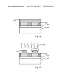
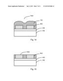
[0045] As shown in FIG. 14, a partially formed resistive switching device 1400 is illustrated. Partially formed resistive switching device 1400 can be fabricated according to steps in FIGS. 2-7. The method includes subjecting second dielectric material 702 to a planarization process to expose a surface region 1502 of first electrode 602. The planarization process can be a chemical mechanical polishing process or an etch back process, or a combination. In certain embodiments, the planarization process can use the first electrode material as an etch stop. In other embodiments, etch stop material can be implemented to maintain an integrity of first electrode surface 1502.
[0046] In various embodiments, the alternative method includes forming a resistive switching material 1602 overlying exposed surface region 1502 of first electrode structure 602 and second dielectric material 702, which has been planarized. Resistive switching material 1602 can be a non-conductive material characterized by an electric resistance depending on an electric field present in the resistive switching material. In various embodiments, resistive switching material 1602 can be an amorphous silicon material having an intrinsic semiconductor characteristic or intrinsic amorphous silicon material hereafter. The intrinsic semiconductor characteristic is maintained by not intentionally doped the amorphous silicon material during deposition or after deposition, as discussed in detail, above.
[0047] Referring to FIG. 17, the alternative method includes subjecting a resistive switching material to a pattern and etch process 1704 to form a resistive switching material structure 1702. Resistive switching material structure 1702 can be configured as a pillar stricture overlying the first electrode structure 602 and maintaining an electric and physical contact with first electrode structure 602 in various embodiments. Resistive switching material structure 1702 includes a vertical wall region 1706, as shown.
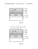
[0048] In various embodiments, the alternative method forms a third dielectric material 1802 overlying resistive switching material structure 1702 including vertical side wall region 1706.
[0049] Third dielectric material can be a silicon oxide material deposited using a deposition process selected from a chemical vapor deposition process, a spin on glass (SOG), and a physical vapor deposition process including a combination thereof. Other suitable dielectric material may be used depending on the application.
[0050] Referring to FIG. 19, the alternative method forms a first material 1902 in a first material region in a vicinity of the vertical side wall region as illustrated. First material 1902 is derived from an interaction of the resistive switching material (for example, the intrinsic amorphous silicon material) and the third dielectric material (for example, the silicon oxide material) in various embodiments.
[0051] The alternative method forms a second electrode material 2002 overlying at least resistive switching material structure 1702 and first material region 1902 as shown in FIG. 20. For intrinsic silicon material as the resistance switching material, second electrode material 2002 can be an active metal material selected from silver, gold, palladium, platinum, copper, aluminum, nickel, zinc, and others. Second electrode material 2002 may be deposited using techniques such as physical vapor deposition process, chemical vapor deposition process, electrochemical deposition (for example, electroplating, electroless plating, and others).
[0052] In various embodiments, second electrode material 2002 is subjected to a pattern and etch process to form a second electrode structure 2102, as shown in FIG. 21. Second electrode structure 2102 is configured to overlie resistive switching material structure 1702 as well as first material region 1902 in various embodiments.
[0053] In various embodiments, first material region 1902 is configured as a path for an active metal material region to form when an electric field is applied. The electric field may be a first voltage having a magnitude no less than a first threshold voltage applied to the second electrode. The first voltage is a positive voltage applied to the second electrode with respect to the first electrode in various embodiments. The active metal material 1702 region includes a filament structure comprising one or more active metal material particles. The filament structure is further characterized by a first distance between the one or more active material particles and a second distance between the filament structure and the first electrode.
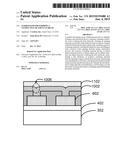
[0054] As shown in FIG. 21, first electrode structure 602, resistive switching material structure 1702 including first material region 1902, and second electrode structure 2102 form a resistive switching device 2104 for a non-volatile memory device in various embodiments. In a programming operation (for example upon application of a positive voltage to second electrode 2102 with respect to first electrode 602), the filament structure extends towards the first electrode structure and cause the resistive switching device to change from a high resistance state (bit value "0") to a low resistance state (bit value 1). After programming, a negative voltage applied to second electrode 2102 in an erase operation would cause the filament structure to retract and cause the resistive switching device to be in the high resistance state. The erase voltage can have substantially a same amplitude as the programming voltage or can also be different depending on the implementation. Again, for intrinsic amorphous silicon material as the resistive switching material and silver as the active metal material, the programming voltage is typically no greater than 8 volts and can range from about 2 volts to 6 volts depending on the device dimension, and others. Resistive switching device 2104 is characterized by a good data retention (maintaining respective resistance states after removal of programming or erase voltage) and high endurance (ability to cycle).
[0055] The present application has been described using intrinsic amorphous silicon material as the resistive switching material, embodiments according to the present invention can be applied to other resistive switching devices where the switching mechanism is base on a conductive filament formed in a resistive switching material as would be obvious to one skilled in the art.
[0056] Some representative claims are as follows:
[0057] 26. A method of forming a resistive switching device for a non-volatile memory device, comprising:
[0058] providing a substrate having a surface region;
[0059] forming a first dielectric material overlying the surface region of the substrate;
[0060] forming a first electrode structure overlying the first dielectric material;
[0061] forming s resistive switching material structure overlying the first electrode, the resistive switching material comprising a vertical side wall region;
[0062] forming a second dielectric material overlying the resistive switching material structure including the vertical side wall region;
[0063] forming a first material derived from the resistive switching material and the second dielectric material in a first material region in a vicinity of the vertical side wall region; and
[0064] forming a second electrode structure overlying the resistive switching material structure including the first material region.
[0065] 27. The method of claim 26 wherein the substrate comprises a semiconductor material selected from monocrystalline silicon, silicon on insulator (SOI), silicon germanium, and polycrystalline silicon.
[0066] 28. The method of claim 26 wherein the first dielectric material is selected from: silicon oxide, silicon nitride, a dielectric stack of alternating layers of silicon oxide and silicon nitride (ONO), a high K dielectric material, a low K dielectric material, and a spin on glass material.
[0067] 29. The method of claim 26 wherein the resistive switching material structure comprises an amorphous silicon material having an intrinsic semiconductor characteristic.
[0068] 30. The method of claim 26 wherein the second dielectric material comprises a silicon oxide material deposited using a deposition process selected from a chemical vapor deposition process, a spin on glass (SOG), and a physical vapor deposition process and a combination thereof.
[0069] 31. The method of claim 26 wherein the second electrode structure comprises an active metal material selected from silver, gold, palladium, platinum, copper, aluminum, nickel, and zinc.
[0070] 32. The method of claim 26 wherein the active metal material forms an active metal material region in a portion of the first material region upon application of a first voltage having an magnitude no less than a first threshold voltage to the second electrode.
[0071] 33. The method of claim 32 wherein the active metal material region comprises a filament structure, the filament structure comprising one or more active metal material particles.
[0072] 34. The method of claim 32 wherein the first voltage is a positive voltage applied to the second electrode with respect to the first electrode.
[0073] 35. The method of claim 26 wherein the first material region provides a path for forming the active metal material region.
[0074] 36. A resistive switching device for a non-volatile memory device, comprising:
[0075] a first electrode structure;
[0076] a resistive switching material structure comprising a resistive switching material having a vertical side wall region overlying the first electrode;
[0077] a dielectric material overlying the resistive switching material structure including the vertical side wall region;
[0078] a first material region comprising a first material configured in a vicinity of the vertical side wall region, the first material being formed from the dielectric material and the resistive switching material; and
[0079] a second electrode structure overlying the resistive switching material structure and overlying the first material region.
[0080] 37. The device of claim 36 wherein the first electrode structure comprises a semiconductor material.
[0081] 38. The device of claim 36 wherein the resistive switching material comprises an amorphous silicon material having an intrinsic semiconductor characteristic.
[0082] 39. The device of claim 36 wherein the dielectric material comprises a silicon oxide material.
[0083] 40. The device of claim 36 wherein the second electrode structure comprises an active metal material selected from silver, gold, palladium, platinum, copper, aluminum, nickel, and zinc.
[0084] 41. The device of claim 36 wherein the active metal material forms an active material region derived from the second electrode structure at least in the first material region upon application of a first positive voltage to the second electrode structure.
[0085] 42. The device of claim 36 wherein the first material region provides a path for the active metal material upon application of the first voltage to cause the resistive switching device to change from a high resistance state to a low resistance state.
[0086] Though the present invention has been described using various examples and embodiments, it is also understood that the examples and embodiments described herein are for illustrative purposes only and that various modifications or alternatives in light thereof will be suggested to persons skilled in the art and are to be included within the spirit and purview of this application and scope of the appended claims.
User Contributions:
Comment about this patent or add new information about this topic:
| People who visited this patent also read: | |
| Patent application number | Title |
|---|---|
| 20150153310 | TURBINE BLADE TESTING DEVICE AND TESTING METHOD THEREOF |
| 20150153309 | BASE-BY-BASE RATCHETING OF DNA/RNA IN A Y-SHAPED NANOCHANNEL |
| 20150153308 | CONTINUOUS CELL DETECTION BY ISOTACHOPHORESIS |
| 20150153307 | SYSTEM FOR RAPID ELECTROPHORESIS BINDING METHOD AND RELATED KITS AND COMPOSITIONS |
| 20150153306 | MINI-GEL COMB |
Images included with this patent application:
 |  |
 |  |
 |  |
 |  |
 |  |
 |  |
| New patent applications in this class: | |
| Date | Title |
|---|---|
| 2022-09-08 | Shrub rose plant named 'vlr003' |
| 2022-08-25 | Cherry tree named 'v84031' |
| 2022-08-25 | Miniature rose plant named 'poulty026' |
| 2022-08-25 | Information processing system and information processing method |
| 2022-08-25 | Data reassembly method and apparatus |