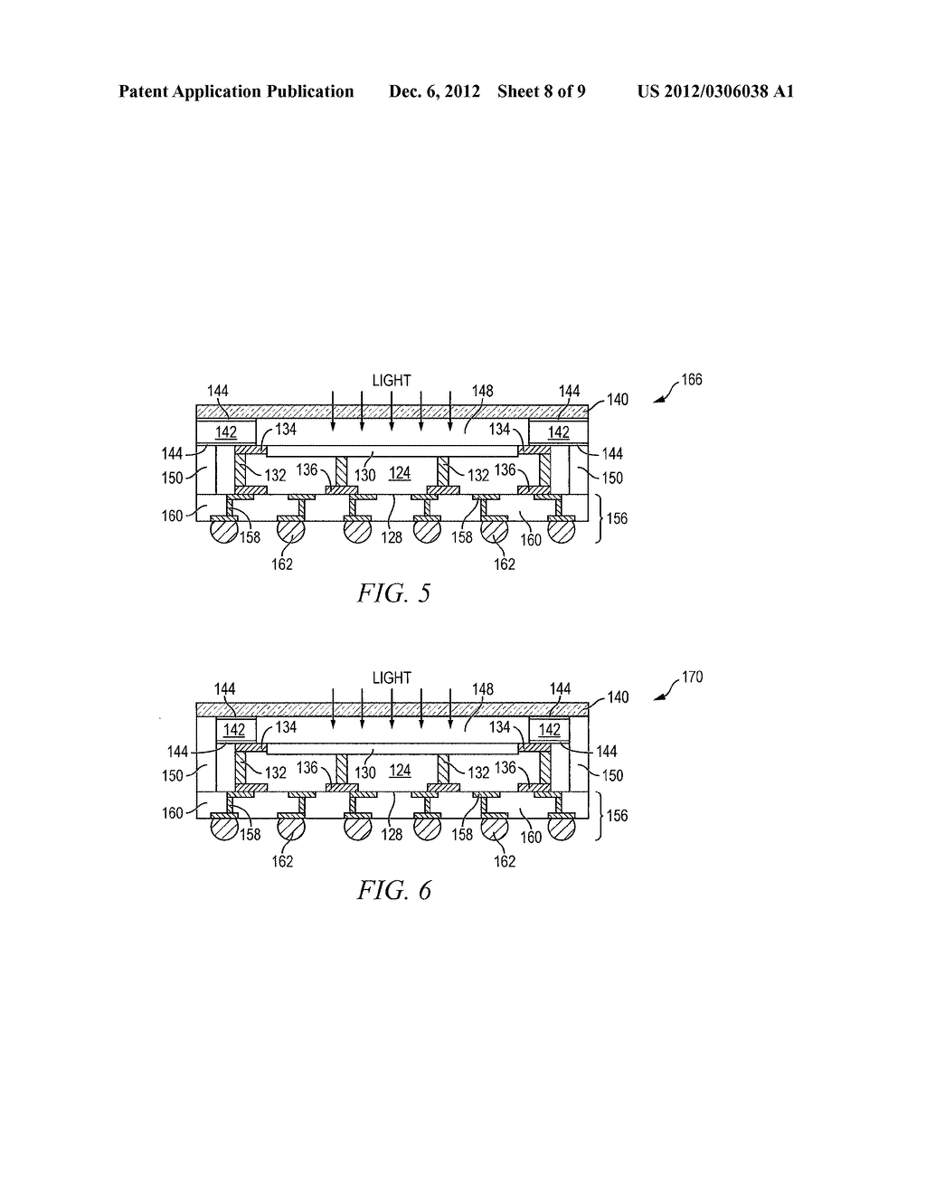
Semiconductor Device and Method of Forming EWLB Semiconductor Package with Vertical Interconnect Structure and Cavity Region - diagram, schematic, and image 09
Back to Semiconductor Device and Method of Forming EWLB Semiconductor Package with Vertical Interconnect Structure and Cavity Region , All Patents .