Process Flow to Reduce Hole Defects in P-Active Regions and to Reduce Across-Wafer Threshold Voltage Scatter - diagram, schematic, and image 04
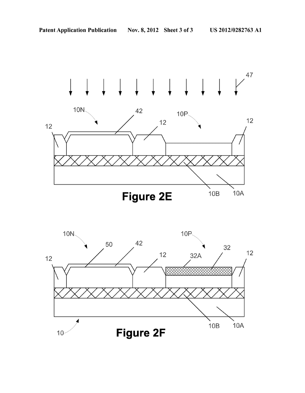
Back to Process Flow to Reduce Hole Defects in P-Active Regions and to Reduce Across-Wafer Threshold Voltage Scatter , All Patents .