Semiconductor Device and Method of Laser-Marking Laminate Layer Formed Over EWLB With Tape Applied to Opposite Surface - diagram, schematic, and image 09
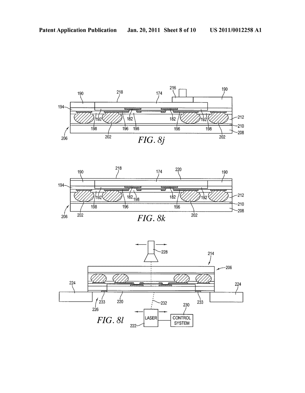
Back to Semiconductor Device and Method of Laser-Marking Laminate Layer Formed Over EWLB With Tape Applied to Opposite Surface , All Patents .