Patent application title: HARMONIC DISPLACEMENT REDUCTION
Inventors:
Fred O. Barthold (Leucadia, CA, US)
IPC8 Class: AH02M132FI
USPC Class:
Class name:
Publication date: 2015-07-09
Patent application number: 20150194874
Abstract:
Reducing voltage excursions in a circuit comprises: performing resonant
commutation, including transferring, via a first set of one or more
diodes, energy stored by a set of one or more parasitic inductances to a
set of one or more capacitors; and performing recovery-to-load, including
discharging energy stored in the set of one or more capacitors via a
second set of one or more diodes, through the set of one or more
parasitic inductances to a load of the circuit.Claims:
1. A method of reducing voltage excursions in a circuit, comprising:
performing resonant commutation, including transferring, via a first set
of one or more diodes, energy stored by a set of one or more parasitic
inductances to a set of one or more capacitors; and performing
recovery-to-load, including discharging energy stored in the set of one
or more capacitors via a second set of one or more diodes, through the
set of one or more parasitic inductances to a load of the circuit.
2. The method of claim 1, wherein the resonant commutation is performed in a first state, and the recovery-to-load is performed in a second state.
3. The method of claim 1, further comprising performing DC-DC power conversion.
4. The method of claim 1, wherein the energy is stored by the set of one or more parasitic inductances while a first switch in a converter is on and a second switch in a converter is off.
5. The method of claim 1, wherein performing resonant commutation includes switching a is first switch in a converter from on to off while keeping a second switch in the converter off.
6. The method of claim 5, wherein switching the first switch from on to off causes a current to cease flowing through the switch and to be commutated through a diode to charge a capacitor.
7. The method of claim 5, wherein performing recovery-to-load includes switching the second switch on while keeping the first switch off.
8. A harmonic displacement reduction circuit comprising: a first set of one or more diodes coupled to a set of one or more capacitors, and a second set of one or more diodes coupled to the set of one or more capacitors; wherein the first set of one or more diodes, the set of one or more capacitors, and the set of one or more diodes are configured to: perform resonant commutation, including to transfer, via the first set of one or more diodes, energy stored by a set of one or more parasitic inductances to the set of one or more capacitors; and perform recovery-to-load, including to discharge energy stored in the set of one or more capacitors via the second set of one or more diodes, through the set of one or more parasitic inductances to a load of a second circuit.
9. The circuit of claim 8, wherein the set of one or more parasitic inductances comprises an interstitial parasitic inductance of magnetic windings of an inductor.
10. The circuit of claim 8, wherein the set of one or more capacitors include COG dielectric.
11. A power converter circuit, comprising: a converter portion comprising a set of one or more parasitic inductances; and a harmonic displacement reduction (HDR) portion coupled to the converter portion, the HDR portion comprising a first set of one or more diodes, a second set of one or more diodes, and a set of one or more capacity. ors, the HDR portion being configured to: perform resonant commutation, including transferring, via the first set of one or more diodes, energy stored by the set of one or more parasitic inductances to the set of one or more capacitors; perform recovery-to-load, including discharge energy stored in the set of one or more capacitors via the second set of one or more diodes, through the set of one or more parasitic inductances to a load of the power converter circuit.
12. The power converter circuit of claim 11, wherein the converter portion is a DC-DC converter.
13. The power converter circuit of claim 11, wherein the converter portion is an isolated, multi-phase boost derived DC-DC converter.
14. The power converter circuit of claim 11, wherein the energy is stored by the set of one or more parasitic inductances while a first switch in a converter is on and a second switch in a converter is off.
15. The power converter circuit of claim 11, further comprising a first switch and a second switch, and wherein the HDR portion's performance of resonant commutation includes switching the first switch from on to off while keeping the second switch in the converter off.
16. The power converter circuit of claim 15, wherein the switching the first switch from on to off causes a current to cease flowing through the switch and to be commutated through a diode to charge a capacitor.
17. The power converter circuit of claim 15, wherein the HDR portion's performance of recovery-to-load includes switching the second switch on while keeping the first switch off.
Description:
CROSS REFERENCE TO OTHER APPLICATIONS
[0001] This application claims priority to U.S. Provisional Patent Application No. 61/925,511 entitled HARMONIC DISPLACEMENT REDUCTION OF SOURCED ALTERNATING CURRENTS FROM THE ISOLATED, MULTI-PHASE, BUCK-BOOST CONVERTER filed Jan. 9, 2014 which is incorporated herein by reference in its entirety for all purposes.
BACKGROUND OF THE INVENTION
[0002] Magnetic field coupling is inherently an imperfect process. The imperfection causes "leakage." Specifically, the interstitial and uncoupled parasitic field element that exists as an inductive energy storage device (LI2) enables leakage energy. For example, power converters often have leakage magnetic fields which cause undesirable voltage excursions and loss in efficiency. Existing techniques to contain the leakage magnetic fields typically have substantial transactional loss due to the use of resistive or reactive elements.
BRIEF DESCRIPTION OF THE DRAWINGS
[0003] Various embodiments of the invention are disclosed in the following detailed description and the accompanying drawings.
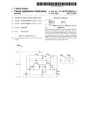
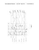
[0004] FIG. 1A is a block diagram illustrating an embodiment of a power converter circuit with leakage.
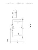
[0005] FIG. 1B is a block diagram illustrating an embodiment of a DC-DC converter comprising a HDR circuit.
[0006] FIG. 2 illustrates a set of time-based wave forms illustrating voltages and currents at various locations on circuit 150 of FIG. 1B.
[0007] FIG. 3 is a flowchart illustrating an embodiment of an LDC/CDL process.
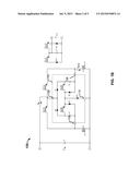
[0008] FIG. 4 illustrates an embodiment of a two-phase, three magnetic, Sepic-fed buck converter 400.
DETAILED DESCRIPTION
[0009] The invention can be implemented in numerous ways, including as a process; an apparatus; a system; a composition of matter; a computer program product embodied on a computer readable storage medium; and/or a processor, such as a processor configured to execute instructions stored on and/or provided by a memory coupled to the processor. In this specification, these implementations, or any other form that the invention may take, may be referred to as techniques. In general, the order of the steps of disclosed processes may be altered within the scope of the invention. Unless stated otherwise, a component such as a processor or a memory described as being configured to perform a task may be implemented as a general component that is temporarily configured to perform the task at a given time or a specific component that is manufactured to perform the task. As used herein, the term `processor` refers to one or more devices, circuits, and/or processing cores configured to process data, such as computer program instructions.
[0010] A detailed description of one or more embodiments of the invention is provided below along with accompanying figures that illustrate the principles of the invention. The invention is described in connection with such embodiments, but the invention is not limited to any embodiment. The scope of the invention is limited only by the claims and the invention encompasses numerous alternatives, modifications and equivalents. Numerous specific details are set forth in the following description in order to provide a thorough understanding of the invention. These details are provided for the purpose of example and the invention may be practiced according to the claims without some or all of these specific details. For the purpose of clarity, technical material that is known in the technical fields related to the invention has not been described in detail so that the invention is not unnecessarily obscured.
[0011] FIG. 1A is a block diagram illustrating an embodiment of a power converter circuit with leakage. Circuit 100 is a two-phase, single magnetic, buck-boost converter. EIN provides a direct current (DC) source. The DC source is converted by circuit 100 into AC so that the current can be transformed. The current is then converted back into DC, as output EOUT. The converter circuit 100 includes two switches Q1 and Q1' that are switched using sequential switching signals, and alternating current (AC) is generated. Inductive windings labeled T2-A, T2-A', T2-C and T2-C' cause leakage. For example, when Q1 is switched on, a current flows in T2-A, causing leakage energy (LI2) to be stored. When Q1 switches off, the leakage energy is released to switches Q1 and Q1'. The leakage energy can damage switches Q1 and Q1' and therefore should be contained. Existing techniques to contain the leakage energy typically employ resistive (dissipative) or reactive (pseudo-lossless) means. The former involves inserting resistors to dissipate the leakage energy, and the latter involves adding inductors or capacitors to redirect energy to the energy source EIN. In either case, the leakage energy is lost due to dissipation or transaction and not delivered to the load.
[0012] A circuit implementing an LDC/CDL sequence to provide resonant commutation and recovery-to-load functions is used to contain or capture the leakage energy and redirect the leakage energy to the load. As used herein, resonant commutation refers to redirecting a current and changing its path (e.g., from a switch to one or more diodes and/or one or more capacitors) at a commutation interval that is determined by the circuit's resonant frequency. Embodiments of LDC/CDL circuits (also referred to as a Harmonic Displacement Reduction (HRD) circuits) coupled to isolated, multi-phase boost derived DC-DC converters and the operations of the LDC/CDL circuits are described. As used herein, isolated means that there is an electrical barrier separating the input and output. In a multi-phase converter, switches are turned on and off according to a switching sequence. In some embodiments, current only flows through one switch at a time.
[0013] The HRD circuit performs resonant commutation and recovery-to-load of the energy content in the magnetic and circuit inductive parasitics in the isolated, multi-phase boost derived DC-DC converter topologies (e.g., buck-boost, flyback, Sepic, Sepic-fed buck, etc.) in either continuous or discontinous mode. The boost derived DC-DC converter topologies have the common characteristic of having a D term in the denominators of their respective transfer functions. Several two-phase examples are shown below, although the technique is generally applicable to N-phase boost derived DC-DC converters (N being an integer>1).
[0014] The HRD circuit delivers the leakage energy to the load (Eout) of the converter, and accomplishes the following in conjunction with the DC-DC converters: (1) establishment of magnetic and circuit inductive parasitics as parameters of utility; (2) functional elimination of the primary-to-secondary current commutation interval; (3) reduction in volume and losses in the power magnetic structure; (4) compelling simplification of the power magnetic construction; (5) reduction of primary switch voltage stress to the near theoretical; (6) reduction of the peak-to-peak and rms currents in the windings, rectifiers and filter capacitors; (7) elimination of source pollution by converter commutation currents; (8) reduction of harmonic current spectrum; (9) near zero current and zero voltage switching of recovery to load current component; and (10) an overall reduction in power component voltage, current, and thermal requirements.
[0015] The HRD circuit carries out a sequence of operations referred to as an LDC/CDL sequence for harmonic displacement commutation and recovery-to-load of inductive parasitic current. As used herein, L=parasitic inductance, C=discrete capacitance, D=diode rectifiers, 1/(2π {square root over (LC)})=harmonic frequency, I=current in parasitic inductance. In a converter topology including the HRD circuit, the LDC/CDL sequence works as follows: in a first state during in the LDC portions of the sequence, the leakage energy from parasitic inductive windings (L) is commutated (redirected) via one or more diodes (D) to one or more capacitors (C). Subsequently, in a second state during the CDL part of the sequence, the energy stored in the one or more capacitors (C) is directed to the load via the one or more diodes (D) and the inductor (L).
[0016] The diode rectifier function of this current commutation sequence may be accomplished by a dedicated active switch (e.g., a field effect transistor (FET), or any other appropriate switching device), when timing and losses so dictate. In some embodiments, the use of appropriate dielectric (e.g., COG dielectric) in the discrete capacitance insures harmonic frequency stability as well as minimum loss. The energy processed through C is (I {square root over (L/C)})2Cf, where f is the converter frequency in Hz. The transaction loss is determined by the loss characteristics of L, D, C and attendant interconnects. The power switch drain voltage excursion is [EIN+EOUT+(0.5I {square root over (L/C)})]. This LDC/CDL sequence may be implemented in various circuit embodiments to provide resonant commutation (through the LDC sequence) and recovery-to-load (through the CDL sequence) of inductive parasitic energy (LI2) in the isolated, multi-phase, boost derived DC-DC converter topologies.
[0017] FIG. 1B is a block diagram illustrating an embodiment of a DC-DC converter comprising a HDR circuit. In FIG. 1A, connections 104-110 illustrate connection points that can be connected to a HDR circuit. In FIG. 1B, the converter shown in FIG. 1A is connected with an embodiment of a HDR circuit 152 at connection points 104-110. Specifically, the HDR circuit includes a set of inductors T2-B and T2-B' that are magnetically coupled with T2-A' and T2-A, a set of capacitors C2 and CT, and diodes D1, D1', D2, D2', and D3.
[0018] Switches Q1 and Q1' are controlled by a controller that sends out control signals (e.g., clock signals) to turn the switches on and off. The inductors, capacitors, and diodes are configured to perform the LDC/CDL sequence which is described in greater detail below. The HDR circuit accepts alternating currents generated based on a DC current source Ein. By performing the LDC/CDL sequence, the HDR circuit achieves harmonic displacement reduction of AC sourced from converter 100.
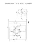
[0019] FIG. 2 illustrates a set of time-based wave forms illustrating voltages and currents at various locations on circuit 150 of FIG. 1B.
[0020] Wave forms 202 and 204 illustrate the drain voltages across switches Q1 and Q1', respectively. Since the circuit has a two-phase configuration, Q1 and Q1' are switched on and off in an alternating pattern. In particular, power switch drain voltage excursion for Q1 and Q1' is limited to [EIN+EOUT+(0.5I {square root over (L/C)})] (see 216 and 218), which is small compared to that of circuit 100.
[0021] Waveform 206 illustrates the current activities in diodes D1, D2, and D3.
[0022] Waveform 208 illustrates the current of IIN.
[0023] Waveforms 210 and 212 illustrate the drain current in Q1 and Q1', respectively.
[0024] Waveform 214 illustrates the capacitor voltages of C2 and CT, which are identical. The voltages of C2 and C2' are due to current being transferred to C2 and C2'. The energy is stored on the capacitors until Q1' is switched on, at which time the energy is discharged in a half cycle of resonance. Thus, compared with the charging of the current, the discharging of current is accomplished through the same L and C values, is of twice the duration, but only half the amplitude.
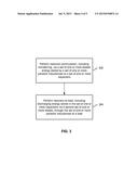
[0025] FIG. 3 is a flowchart illustrating an embodiment of an LDC/CDL process. Process 300 can be performed by a HDR circuit such as 152 of FIG. 1B or 402 of FIG. 4. The process is explained in connection with FIG. 1B and FIG. 2.
[0026] At 302, resonant commutation is performed. In some embodiments, resonant commutation includes transferring, via a first set of one or more diodes, energy stored by a set of one or more parasitic inductances to a set of one or more capacitors. The parasitic inductances and the capacitors have a resonant frequency, which determines how long the commutation interval lasts.
[0027] Referring to the example circuit of FIG. 1B, when Q1 is switched on, the drain voltage of Q1 is low, a current flows through Q1 and through T2-A, and energy is stored (this is the L portion of the LDC process). Note that the parasitic inductance L does not necessarily exist as a physical component, but is a measure of the coupling properties of inductor T2 because the parasitic inductance L exists as interstitial parasitic inductance of the magnetic windings of T2. When Q1 is switched off, the current that was previously flowing through Q ceases to flow through Q1, and is commutated through D1 (D portion of LDC) and charges C2 (C portion of LDC). Since CT is in parallel with C2, any energy transferred to C2 is also transferred to CT.
[0028] Referring to FIG. 2, the L portion of the LDC process takes place immediately prior to time t0, when switch Q1 is on and switch Q1' is off. Q1 draws current, and energy is stored in the parasitic inductances. The D and C portion of the LDC process takes place starting at time t0, when switch Q1 is switched off and switch Q1' remains off. The drain voltage of Q1 jumps, as illustrated by portion 216 of waveform 202. The current flows through D1' and D2 to charge capacitors C2 and CT, as illustrated by 240 of waveform 206. Since 240 is a quarter sine at the resonant frequency, the circuit is said to commutate at a quarter cycle of the resonant period. The voltage across the capacitors does not increase in a linear fashion. The rate of increase is greatest when the current of waveform 206 is the greatest. Voltage Eout increases until the capacitors are charged at time t1, at which time energy is contained in the capacitors and the circuit enters a quiescent state as shown in the portion labeled 226 in waveform 214. Neither switch Q1 nor switch Q1' is turned on during the quiescent period. As shown in waveforms 208, 210, and 212, respectively, input current IN, drain current Q1, and drain current Q1' are all zero during the quiescent period. The drain voltages for switches Q1 and Q1' are both at a set level (Ein+Eout).
[0029] Returning to process 300 of FIG. 3, at 304, recovery-to-load is performed. In some embodiments, recovery-to-load includes discharging energy stored in the set of one or more capacitors via a second set of one or more diodes, through the set of one or more parasitic inductances to a load.
[0030] Referring to the example circuit of FIG. 1B, on the next interval, Q1' is switched on, energy is discharged from C2 and CT (the C portion of the CDL process) via D3 (the D portion of CDL process), which energy is transferred from the primary windings to the secondary windings T2-C (the L portion of CDL) and thus transferred to the load.
[0031] Referring to FIG. 2, the CDL process starts at time t2, when Q1' is switched on while Q1 remains off. As shown in waveform 204, the drain voltage of Q1' drops to 0 at this time. The energy stored in capacitors C2 and CT is discharged through D3 to load. This is the commutation current (also referred to as redirected current), which is labeled 220 in waveform 206. Since 220 is a half sine wave at the resonant frequency (with an amplitude that is half of 240), the circuit is said to deliver to load at a half cycle. In addition, as shown in waveform 208, there is a current 222 extracted from current source EIN. The drain current Q1', which is the sum of the commutation current and the sourced current, is labeled 224 in waveform 212. Capacitors C2 and CT are discharged, and voltage across the capacitors decreases, as shown in the portion labeled 226 in waveform 214. At time t3, the capacitors are discharged until no more current can be drained to the load from the capacitors, as shown in the portion labeled 236 in waveform 214. At this point, current is only drained from the source, as waveform 208 EIN shows. In waveform 214, the voltage across the capacitors drops below EOUT, by an amount that depends on the values of the parasitic inductance L and capacitance C. The CDL process completes.
[0032] Process 300 is repeated on the next half-cycle. Prior to time t4, Q1' continues to draw current and energy is stored in parasitic inductances. At time t4, switch Q1' is switched off, and switch Q1 remains off. The drain voltage of Q1' jumps, as illustrated by portion 218 of waveform 204. The current flows through D1' and D2 to charge capacitors C2 and C2' (the LDC process), as illustrated by portion 228 of waveform 206. Voltage Eout increases until the capacitors are charged. At this point (time t5), the circuit enters a quiescent state.
[0033] At time t6, switch Q1 is switched on while Q1' remains off. As shown in waveform 204, the drain voltage of Q1 drops to 0 at this time. The energy stored in capacitors C2 and CT is discharged through D3 to load (the CDL process). The commutation current (also referred to as redirected current) is labeled 230 in waveform 206. In addition, as shown in waveform 208, there is a current 232 extracted from current source EIN. The drain current Q1, which is the sum of the commutation current and the sourced current, is labeled 234 in waveform 210. Capacitors C2 and CT are discharged, and voltage EOUT across the capacitors decreases until the capacitors are discharged, as shown in the portion labeled 236 in waveform 214.
[0034] At time t7, the capacitors are discharged until no more current can be drained to the load from the capacitors. At this point, current is only drained from the source, as waveform 208 EIN shows.
[0035] A full switching cycle completes and a new cycle repeats at t8.
[0036] In converter circuits with FET-based switches Q1 and Q1', FET losses are directly related to the drive requirements, and loss current characteristics are directed to voltage rating. Thus, it is generally preferable to use FETs with lower voltage rating. The reduction of excursion voltage permits the use of devices with lower voltage ratings and better characteristics. For example, assume that the maximum input voltage E'in is 72v and the maximum output voltage Eout is 24v, which add up to 96v. The HDR circuit can keep the excursion portion of the output voltage to under 4 volts, allowing 100v FET to be used for Q1 and Q2 in the converter circuit. Without the HDR circuit to reduce the excursion voltage, 150v FET or even 200v FET would have to be used.
[0037] Other forms of HDR circuit can be designed to be coupled to other power converters to perform the LDC-CDL process. FIG. 4 illustrates an embodiment of a two-phase, three magnetic, Sepic-fed buck converter 400. An HDR 402 is coupled to converter 400 at connection points 404, 406, 408, and 410. In this example, the structure of HDR 402 is different from that of HDR circuit 152 in FIG. 1B in that HDR 402 utilizes the windings in converter 400 as the L portion of the LDC/CDL process, while of HDR 152 includes additional windings T2-B and T2-B' (L portion). The windings are used to provide the conductive path for the CDL process. When Q1 (or Q1') is turned on, C2 and CT are discharged through T2-B' and T2-B and current goes through D3. In a 3 magnetic device such as 400, there is no need to add additional magnetic windings to the HDR circuit because the functions of T2-B' and T2-B of HDR 152 are performed by T1-B and T1-B' in converter 400. In other words, the existing windings in the converter provide the conductive path for the CDL process. The windings are merged into the structure of a single magnetic winding.
[0038] In various embodiments, depending on the power converter circuit configuration, the HDR circuit may be configured differently. For the same power converter, different HDR circuit configurations are possible. Besides the examples described herein, there are other ways to connect the diodes and capacitors in the HDR circuit as well as multiple ways to connect the HDR circuit to the power converter to accomplish the LDC-CDL sequence.
[0039] One skilled in the art can design a HDR by following the following HDR design process which is used in some embodiments:
[0040] The value of leakage is computed using known techniques (e.g., according to the techniques described by Rueben Lee, "Electronic Transformers and Circuits" (second edition), John Wiley & Sons, New York, N.Y., 1961.) to determine the L term. In the example of FIG. 1B, L is the parasitic inductance between T2-A and T2-C (or T2-A' and T2-C'). In the example of FIG. 4, parasitic inductance L is equivalently distributed in the discrete windings 420-442.
[0041] Given L and the harmonic frequency desired 1/(2π {square root over (LC)}), the capacitance C is determined. The harmonic frequency 1/(2π {square root over (LC)}) is chosen by the designer, and should be as low as possible, while minimizing energy losses. Some tradeoffs are made in the choice of the harmonic frequency, as a lower value (which reduces the voltage excursion) requires a bigger C value, but a bigger C results in higher transaction losses because the interval of conduction of the diodes is longer. There is compromise of transactional losses and containment of the voltage excursion. Further, the value of C should be selected as appropriate for the dielectric material selected to implement the circuit. In some embodiments, C is selected to be within the range of values appropriate for COG dielectric. In some embodiments, the harmonic frequency is selected to be 5 times the switching frequency. In some embodiments, if the C value determined is unsatisfactory, the magnetic windings are redesigned (e.g., changing winding sequences, changing the aspect ratio of the window, interleaving the windings, etc.) to achieve a different L that would allow the selection of a more appropriate C (e.g., a C having a capacitance value that leads to lower voltage excursion, lower transactional loss, and/or is within the range supported by the dielectric.)
[0042] The diodes (D) are selected based on transactional losses, which depends on the amount of current flowing through the diodes. Once L and C are chosen, the amount of current flowing through the diode can be predicted according to
Δ I = V L t ##EQU00001##
A diode must be able to handle the predicted amount of current.
[0043] There are different ways to connect inductors, diodes, etc. to accomplish the LDC/CDL sequence. Generally, the leakage energy is stored in the parasitic inductance L and can be transferred via a diode to a capacitor C. After a quiescent period, the energy stored in the capacitor C is transferred via another diode through the same inductance L to the load. A circuit that provides resonant commutation in that L and C have a resonant frequency (harmonic frequency), and performs displacement in that at some point in time the circuit performs the LDC process, and at a later point in time the circuit performs CDL process.
[0044] Although the foregoing embodiments have been described in some detail for purposes of clarity of understanding, the invention is not limited to the details provided. There are many alternative ways of implementing the invention. The disclosed embodiments are illustrative and not restrictive.
User Contributions:
Comment about this patent or add new information about this topic:
Images included with this patent application:
 |  |
 |  |
 |  |
| New patent applications in this class: | |
| Date | Title |
|---|---|
| 2022-09-08 | Shrub rose plant named 'vlr003' |
| 2022-08-25 | Cherry tree named 'v84031' |
| 2022-08-25 | Miniature rose plant named 'poulty026' |
| 2022-08-25 | Information processing system and information processing method |
| 2022-08-25 | Data reassembly method and apparatus |
| New patent applications from these inventors: | |
| Date | Title |
|---|---|
| 2016-04-21 | Planar core with high magnetic volume utilization |
| 2014-11-20 | Planar core with high magnetic volume utilization |
| 2014-10-09 | Planar core-type uniform external field equalizer and fabrication |
| 2009-07-09 | Dc-dc converter |
| 2009-07-09 | Sepic fed buck converter |