Patent application title: METHOD FOR REDUCING MORPHOLOGICAL DIFFERENCE BETWEEN N-DOPED AND UNDOPED POLYSILICON GATES AFTER ETCHING
Inventors:
Zaifeng Tang (Shanghai, CN)
Yukun Lv (Shanghai, CN)
Chao Fang (Shanghai, CN)
Hsusheng Chang (Shanghai, CN)
Hsusheng Chang (Shanghai, CN)
Assignees:
SHANGHAI HUALI MICROELECTRONICS CORPORATION
IPC8 Class: AH01L2128FI
USPC Class:
438703
Class name: Chemical etching combined with coating step plural coating steps
Publication date: 2013-11-28
Patent application number: 20130316539
Abstract:
The present invention discloses a method for reducing the morphological
difference between N-doped and undoped poly-silicon gates after etching,
comprising the following sequential steps: depositing a hard mask layer
on a substrate template having N-doped poly-silicon and undoped
poly-silicon to form an N-doped poly-silicon hard mask layer and an
undoped poly-silicon hard mask layer respectively, and etching the
undoped poly-silicon hard mask layer to make a thickness difference
between the N-doped poly-silicon hard mask layer and the undoped
poly-silicon hard mask layer; depositing an anti-reflection layer, and
etching according to a predetermined pattern until exposing the N-doped
poly-silicon, wherein when the N-doped poly-silicon is exposed, the
undoped poly-silicon is etched to a certain degree; and removing
residuals on the surface of the above formed structure, and etching to
form an N-doped poly-silicon gate and an undoped poly-silicon gate,
respectively.Claims:
1. A method for reducing the morphological difference between the N-doped
and undoped poly-silicon gates after etching comprising the following
sequential steps: Step 1: depositing a hard mask layer on a substrate
template having N-doped poly-silicon and undoped poly-silicon to form an
N-doped poly-silicon hard mask layer and an undoped poly-silicon hard
mask layer respectively, and etching the undoped poly-silicon hard mask
layer to make a thickness difference between the N-doped poly-silicon
hard mask layer and the undoped poly-silicon hard mask layer; the
thickness of the undoped poly-silicon hard mask layer is etched to be
less than that of the N-doped poly-silicon hard mask layer; Step 2:
depositing an anti-reflection layer on the N-doped poly-silicon hard mask
layer and the undoped poly-silicon hard mask layer with different
thicknesses, and etching according to a predetermined pattern until
exposing the N-doped poly-silicon, wherein when the N-doped poly-silicon
is exposed, the undoped poly-silicon is etched to a certain degree; Step
3: removing residuals formed during etching on the surface of the above
structure formed by Step 2, and etching the N-doped poly-silicon and
undoped poly-silicon to form an N-doped poly-silicon gate and an undoped
poly-silicon gate, respectively.
2. The method of claim 1, wherein the thickness difference between the undoped poly-silicon hard mask layer and the N-doped poly-silicon hard mask layer in the Step 1 is related to the etching rate ratio of the hard mask layer and the undoped poly-silicon in the Step 2, as well as the etching rate ratio of the undoped poly-silicon and N-doped poly-silicon in the Step 3.
3. The method of claim 2, wherein the thickness difference between the undoped poly-silicon hard mask layer and the N-doped poly-silicon hard mask layer in the Step 1 is calculated according to the following equation: T HM _ P poly = ER HM _ HM ER Ppoly _ HM × T Ppoly _ etch ##EQU00009## where THM.sub.--.sub.Ppoly is the thickness difference between the undoped poly-silicon hard mask layer and the N-doped poly-silicon hard mask layer in the Step 1, ERHM.sub.--.sub.HM is the etching rate of the hard mask layer in the Step 2, ERPpoly.sub.--.sub.HM is the etching rate of the undoped poly-silicon in the Step 2, TPpoly.sub.--.sub.etch is the etching thickness of the undoped poly-silicon when the N-doped poly-silicon is exposed in the Step 2, and TPpoly.sub.--.sub.etch is calculated according to the following equation: TPpoly.sub.--.sub.etch=TPpoly.sub.--.sub.remain where TPpoly.sub.--.sub.remain is the remaining thickness of the undoped poly-silicon when the etching of the N-doped poly-silicon gate is complete in the conventional technology, and TPpoly.sub.--.sub.remain is calculated according to the following equation: T Ppoly _ remain = T poly - ER Ppoly _ poly ER Npoly _ poly × T poly ##EQU00010## where Tpoly is the total thickness of the N-doped and undoped poly-silicon, ERPpoly.sub.--.sub.poly is the etching rate of the undoped poly-silicon, ERNpoly.sub.--.sub.poly is the etching rate of the N-doped poly-silicon.
4. The method of claim 1, wherein the etching time for etching the undoped poly-silicon hard mask layer is calculated according to the following equation: Time HM _ etch = T HM _ Ppoly ER HM _ HM ##EQU00011## where TimeHM.sub.--.sub.etch is the etching time for etching the undoped poly-silicon hard mask layer in the Step 1, ERHM.sub.--.sub.HM is the etching rate of the hard mask layer in the Step 1, THM.sub.--.sub.Ppoly is the thickness difference between the undoped poly-silicon hard mask layer and the N-doped poly-silicon hard mask layer in the Step 1, and THM.sub.--.sub.Ppoly is calculated according to the following equation: T HM _ P poly = ER HM _ HM ER Ppoly _ HM × T Ppoly _ etch ##EQU00012## Where THM.sub.--.sub.Ppoly is the thickness difference between the undoped poly-silicon hard mask layer and the N-doped poly-silicon hard mask layer in the Step 1, ERHM.sub.--.sub.HM is the etching rate of the hard mask layer in the Step 2, ERPpoly.sub.--.sub.HM is the etching rate of the undoped poly-silicon in the Step 2, TPpoly.sub.--.sub.etch is the etching thickness of the undoped poly-silicon when the N-doped poly-silicon is exposed in the Step 2, and TPpoly.sub.--.sub.etch is calculated according to the following equation: TPpoly.sub.--.sub.etch=TPpoly.sub.--.sub.remain where TPpoly.sub.--.sub.remain is the remaining thickness of the undoped poly-silicon when the etching of the N-doped poly-silicon gate is complete in the conventional technology, and TPpoly.sub.--.sub.remain is calculated according to the following equation: T Ppoly _ remain = T poly - ER Ppoly _ poly ER Npoly _ poly × T poly ##EQU00013## where Tpoly is the total thickness of the N-doped and undoped poly-silicon, ERPpoly.sub.--.sub.poly is the etching rate of the undoped poly-silicon, ERNpoly.sub.--.sub.poly is the etching rate of the N-doped poly-silicon.
Description:
CROSS-REFERENCE TO RELATED APPLICATION
[0001] This application claims the priority benefit of China application serial no. 201210163138.4, filed May 22, 2012. All disclosure of the China application is incorporated herein by reference.
FIELD OF THE INVENTION
[0002] The present invention relates to the field of microelectronic technology, and particularly to a method for improving the morphological difference between N-doped and undoped poly-silicon gates after etching.
BACKGROUND OF THE INVENTION
[0003] In the technology with a critical dimension of 65 nm or less, it is generally required that a poly-silicon gate in the device should be composed of N-doped poly-silicon and undoped poly-silicon. Due to the effect of N-type ion doping, the etching rate of the N-doped poly-silicon is larger than that of the undoped poly-silicon.
[0004] In an automatic end point detection system, the basis for determining the termination of the poly-silicon gate etching is that both the N-doped and undoped poly-silicon gates are completely etched. In case that the etching of the N-doped poly-silicon gate is completed in advance due to its relatively larger etching rate, and the plasma bombardment is still performed in order to etch the undoped poly-silicon gate, the bottom of the N-doped poly-silicon gate will be damaged, thus developing an under-cut. In this process condition, there will be a difference between the N-type and P-type semiconductor devices, which may influence the overall performance of the final product.
[0005] The etching process for the 65 nm and 55 nm scale poly-silicon gate commonly comprises the following steps. Step 1: after growing poly-silicon composed of N-doped poly-silicon and undoped poly-silicon, forming a hard mask layer on the poly-silicon serving as an etching blocking layer and depositing an anti-reflection layer subsequently. Step 2: coating a photoresist and applying photolithography to form a patterned photoresist layer for the poly-silicon gate etching. Step 3: starting the etching process by etching the anti-reflection layer firstly using the patterned photoresist layer as a mask. Step 4: etching the hard mask layer. Step 5: removing the patterned photoresist layer in the etching machine. Step 6: etching the poly-silicon to from a poly-silicon gate. During the etching process for forming the poly-silicon gate, since the etching rate of the N-doped poly-silicon is larger than that of the undoped poly-silicon, a morphological difference will develop between them.
SUMMARY OF THE INVENTION
[0006] The present invention provides a method for improving morphological difference between the N-doped and undoped poly-silicon gates after etching, namely, a method which eliminates the morphological difference between the N-doped poly-silicon gate and the undoped poly-silicon gate after etching due to the larger etching rate of the N-doped poly-silicon than that of the undoped poly-silicon, by forming a relatively thick hard mask layer on the N-doped poly-silicon.
[0007] In order to achieve the above object, the present invention provides a method for reducing the morphological difference between the N-doped and undoped poly-silicon gates after etching comprising the following sequential steps:
[0008] Step 1: depositing a hard mask layer on a substrate template having N-doped poly-silicon and undoped poly-silicon to form an N-doped poly-silicon hard mask layer and an undoped poly-silicon hard mask layer respectively, and etching the undoped poly-silicon hard mask layer to make a thickness difference between the N-doped poly-silicon hard mask layer and the undoped poly-silicon hard mask layer; the thickness of the undoped poly-silicon hard mask layer is etched to be less than that of the N-doped poly-silicon hard mask layer;
[0009] Step 2: depositing an anti-reflection layer on the N-doped poly-silicon hard mask layer and the undoped poly-silicon hard mask layer with different thicknesses, and etching according to a predetermined pattern until exposing the N-doped poly-silicon, wherein when the N-doped poly-silicon is exposed, the undoped poly-silicon is etched to a certain degree;
[0010] Step 3: removing residuals formed during etching on the surface of the above structure formed by Step 2, and etching the N-doped poly-silicon and undoped poly-silicon to form an N-doped poly-silicon gate and an undoped poly-silicon gate, respectively.
[0011] In a preferred embodiment of the present invention, wherein the thickness difference between the undoped poly-silicon hard mask layer and the N-doped poly-silicon hard mask layer in the Step 1 is related to the etching rate ratio of the hard mask layer and the undoped poly-silicon in the Step 2, as well as the etching rate ratio of the undoped poly-silicon and N-doped poly-silicon in the Step 3.
[0012] In a preferred embodiment of the present invention, wherein the thickness difference between the undoped poly-silicon hard mask layer and the N-doped poly-silicon hard mask layer in the Step 1 is calculated according to the following equation:
T HM _ P poly = ER HM _ HM ER Ppoly _ HM × T Ppoly _ etch ##EQU00001##
where THM--Ppoly is the thickness difference between the undoped poly-silicon hard mask layer and the N-doped poly-silicon hard mask layer in the Step 1, ERHM--HM is the etching rate of the hard mask layer in the Step 2, ERPpoly--HM is the etching rate of the undoped poly-silicon in the Step 2, TPpoly--.sub.etch is the etching thickness of the undoped poly-silicon when the N-doped poly-silicon is exposed in the Step 2, and TPpoly--.sub.etch is calculated according to the following equation:
TPpoly--.sub.etch=TPpoly--.sub.remain
where TPpoly--.sub.remain is the remaining thickness of the undoped poly-silicon when the etching of the N-doped poly-silicon gate is complete in the conventional technology, and TPpoly--.sub.remain is calculated according to the following equation:
T Ppoly _ remain = T poly - ER Ppoly _ poly ER Npoly _ poly × T poly ##EQU00002##
where Tpoly is the total thickness of the N-doped and undoped poly-silicon, ERPpoly--poly is the etching rate of the undoped poly-silicon, and ERNpoly--poly is the etching rate of the N-doped poly-silicon.
[0013] In a preferred embodiment of the present invention, the etching time for etching the undoped poly-silicon hard mask layer is calculated according to the following equation:
Time HM _ etch = T HM _ Ppoly ER HM _ HM , ##EQU00003##
where TimeHM--.sub.etch is the etching time for etching the undoped poly-silicon hard mask layer in the Step 1, ERHM--HM is the etching rate of the hard mask layer in the Step 1, THM--Ppoly is the thickness difference between the undoped poly-silicon hard mask layer and the N-doped poly-silicon hard mask layer in the Step 1, and THM--Ppoly is calculated according to the following equation:
T HM _ P poly = ER HM _ HM ER Ppoly _ HM × T Ppoly _ etch , ##EQU00004##
where THM--Ppoly is the thickness difference between the undoped poly-silicon hard mask layer and the N-doped poly-silicon hard mask layer in the Step 1, ERHM--HM is the etching rate of the hard mask layer in the Step 2, ERPpoly--HM is the etching rate of the undoped poly-silicon in the Step 2, TPpoly--.sub.etch is the etching thickness of the undoped poly-silicon when the N-doped poly-silicon is exposed in the Step 2, and TPpoly--.sub.etch is calculated according to the following equation:
TPpoly--.sub.etch=TPpoly--.sub.remain,
where TPpoly--.sub.remain is the remaining thickness of the undoped poly-silicon when the etching of the N-doped poly-silicon gate is complete in the conventional technology, and TPpoly--.sub.remain is calculated according to the following equation:
T Ppoly _ remain = T poly - ER Ppoly _ poly ER Npoly _ poly × T poly ##EQU00005##
where Tpoly is the total thickness of the N-doped and undoped poly-silicon, ERPpoly--poly is the etching rate of the undoped poly-silicon, and ERNpoly--poly is the etching rate of the N-doped poly-silicon.
[0014] The method of the present invention can effectively improve the morphological difference between the N-doped and undoped poly-silicon gates after etching.
BRIEF DESCRIPTION OF THE DRAWINGS
[0015] FIG. 1 is a structural diagram illustrating etching of an undoped poly-silicon hard mask layer in an embodiment of the present invention.
[0016] FIG. 2 is a diagram illustrating the structure in which silicon hard mask layers with different thicknesses have been formed in an embodiment of the present invention.
[0017] FIG. 3 is a diagram illustrating the structure in which an anti-reflection layer has been deposited in an embodiment of the present invention.
[0018] FIG. 4 is a diagram illustrating the structure in which the etching of the hard mask layer is complete in an embodiment of the present invention.
[0019] FIG. 5 is a diagram illustrating the structure in which an N-doped poly-silicon gate and an undoped poly-silicon gate have been formed in an embodiment of the present invention.
DETAILED DESCRIPTION OF THE EMBODIMENTS
[0020] The present invention provides a method for improving morphological difference between the N-doped and undoped poly-silicon gates after etching, namely, a method which eliminates the morphological difference between the N-doped and undoped poly-silicon gates after etching due to the larger etching rate of N-doped poly-silicon than that of undoped poly-silicon, by forming a relatively thick hard mask layer on the N-doped poly-silicon gate.
[0021] The present invention will be described in further details hereinafter by referring to embodiments thereof, so as to provide a better understanding of the present invention. However, these embodiments do no intend to limit the scope of the present invention.
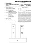
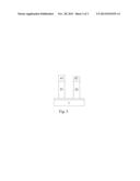
[0022] As shown in FIG. 1, a hard mask layer is deposited on a substrate template 1 comprising N-doped poly-silicon 31 and undoped poly-silicon 32 to form an N-doped poly-silicon hard mask layer 41 and an undoped poly-silicon hard mask layer 42, respectively, and the undoped poly-silicon hard mask layer 42 is etched so as to have a thickness less than that of the N-doped poly-silicon hard mask layer 41. The etching of the undoped poly-silicon hard mask layer 42 can be performed by using a patterned photoresist PR as a mask. The resulting structure is shown in FIG. 2.
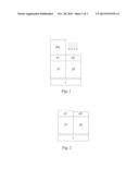
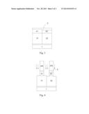
[0023] As shown in FIG. 3, an anti-reflection layer 5 is deposited on the N-doped poly-silicon hard mask layer 41 and the undoped poly-silicon hard mask layer 42 which have different thicknesses. The formed device is etched according to a predetermined pattern until the N-doped poly-silicon 31 is exposed. As shown in FIG. 4, when the N-doped poly-silicon 31 is exposed, the undoped poly-silicon 32 is etched to a certain degree.
[0024] Afterwards, the residuals on the device surface during etching are removed. Then the device is etched to form an N-doped poly-silicon gate 41 and an undoped poly-silicon gate 42, as shown in FIG. 5.
[0025] In the step of etching to form the poly-silicon gates, there is a difference in etching rate between the N-doped poly-silicon 31 and the undoped poly-silicon 32. Therefore, it is necessary to determine the remaining thickness of the undoped poly-silicon to be etched when the etching of the N-doped poly-silicon gate is complete. The remaining thickness is determined according to the etching rate ratio of the undoped poly-silicon and N-doped poly-silicon. In an embodiment, the remaining thickness is calculated according to the following equation:
T Ppoly _ remain = T Poly - ER Ppoly _ poly ER Npoly _ poly × T poly ( 1 ) ##EQU00006##
where TPpoly--.sub.remain is the remaining thickness of the undoped poly-silicon when the etching of the N-doped poly-silicon gate is complete in the conventional technology, Tpoly is the total thickness of the poly-silicon composed of the N-doped and undoped poly-silicon, ERPpoly--poly is the etching rate of the undoped poly-silicon, ERNpoly--poly is the etching rate of the N-doped poly-silicon.
[0026] Since the remaining thickness of the undoped poly-silicon equals to the thickness of the undoped poly-silicon TPpoly--.sub.etch which is required to be etched during the etching of the hard mask layers, then
TPpoly--.sub.etch=TPpoly--.sub.remain (2)
[0027] During the step of etching the hard mask layers, the etching thickness of the hard mask layer on the undoped poly-silicon, i.e., the thickness difference between the undoped poly-silicon hard mask layer and the N-doped poly-silicon hard mask layer THM--Ppoly, is determined according to the etching rate ratio of the hard mask layer and the undoped poly-silicon. In an embodiment, the thickness difference THM--Ppoly is calculated according to the following equation:
T HM _ P poly = ER HM _ HM ER Ppoly _ HM × T Ppoly _ etch ( 3 ) ##EQU00007##
where ERHM--HM is the etching rate of the hard mask layer, and ERPpoly--HM is the etching rate of the undoped poly-silicon.
[0028] From the calculated thickness difference THM--Ppoly and the etching rate of the hard mask layer ERHM--HM, it is possible to calculate the etching time TimeHM--.sub.etch for the hard mask layer located on the undoped poly-silicon. The etching time TimeHM--.sub.etch is calculated according to the following equation:
Time HM _ etch = T HM _ Ppoly ER HM _ HM ( 4 ) ##EQU00008##
[0029] The specific embodiments of the present invention have been described as above, but the present invention is not limited to the embodiments described above, since these embodiments are only exemplary in nature. It is apparent for the skilled in the art that any equivalent modification and substitution fall within the scope of the present invention. Therefore, all equivalent modifications and substitutions without departing from the spirit and scope of the present invention should be covered by the present invention.
User Contributions:
Comment about this patent or add new information about this topic:
| People who visited this patent also read: | |
| Patent application number | Title |
|---|---|
| 20140068186 | METHODS AND APPARATUS FOR DESIGNATING OR USING DATA STATUS INDICATORS |
| 20140068185 | AVOIDING RECALL OPERATIONS IN A TIERED DATA STORAGE SYSTEM |
| 20140068184 | ASSIMILATION OF FOREIGN LUNS INTO A NETWORK STORAGE SYSTEM |
| 20140068183 | SYSTEMS, METHODS, AND INTERFACES FOR ADAPTIVE PERSISTENCE |
| 20140068182 | Storage Virtualization In A Block-Level Storage System |
Images included with this patent application:
 |  |
 |  |
| Similar patent applications: | |
| Date | Title |
|---|---|
| 2013-09-26 | Method for reducing damage to low-k gate spacer during etching |
| 2013-12-05 | Three dimensional microelectronic components and fabrication methods for same |
| 2012-04-26 | Combinatorial plasma enhanced deposition techniques |
| 2012-04-26 | Combinatorial plasma enhanced deposition techniques |
| 2013-11-28 | Surface morphology generation and transfer by spalling |
| New patent applications in this class: | |
| Date | Title |
|---|---|
| 2019-05-16 | Fine line patterning methods |
| 2019-05-16 | Method of forming semiconductor structure |
| 2019-05-16 | Positive photoresist composition, via-forming method, display substrate and display device |
| 2017-08-17 | Pattern forming method |
| 2017-08-17 | Method and apparatus for multi-film deposition and etching in a batch processing system |
| New patent applications from these inventors: | |
| Date | Title |
|---|---|
| 2022-09-01 | Method for manufacturing shallow trench isolation |
| 2022-01-06 | Electrical connector having position holder |
| 2017-01-26 | Method for establishing mapping relation in sti etch and controlling critical dimension of sti |
| 2015-03-05 | Process of manufacturing the gate oxide layer |
| 2014-06-05 | Apparatus for detecting the flatness of wafer and the method thereof |
| Top Inventors for class "Semiconductor device manufacturing: process" | |
| Rank | Inventor's name |
|---|---|
| 1 | Shunpei Yamazaki |
| 2 | Shunpei Yamazaki |
| 3 | Kangguo Cheng |
| 4 | Chen-Hua Yu |
| 5 | Devendra K. Sadana |