Patent application title: LOW NOISE AND LOW POWER VOLTAGE CONTROLLED OSCILLATORS
Inventors:
Mohammad Ardehali (Palo Alto, CA, US)
Assignees:
TagArray, Inc.
IPC8 Class: AH03L7099FI
USPC Class:
327159
Class name: With feedback phase lock loop with digital element
Publication date: 2013-11-14
Patent application number: 20130300476
Abstract:
LC tank and ring-based VCOs are disclosed that each include a
differential pair of transistors for steering a tail current generated by
a current source responsive to a bias voltage. A biasing circuit
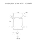
generates the bias voltage such that a transconductance for the
transistors in the differential pairs is inversely proportional to a
resistance.Claims:
1. An LC tank voltage controlled oscillator (VCO) having an output signal
having a frequency responsive to a tuning signal, comprising: a first
inductor and a second inductor, each inductor having a parallel
equivalent resistance; a differential pair of transistors configured to
steer a tail current from a current source transistor, a first transistor
in the differential pair coupled to a power supply node through the first
inductor and a second transistor in the differential pair coupled to the
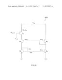
power supply node through the second inductor; and a biasing circuit
configured to generate a bias voltage for the current source transistor
such that a transconductance for the first and second transistors is
proportional to the inverse of the parallel equivalent resistance.
2. The LC tank VCO of claim 1, wherein the biasing circuit includes a first PMOS transistor and a second PMOS transistor in a current mirror configuration.
3. The LC tank VCO of claim 2, wherein the biasing circuit further includes a first NMOS transistor, and wherein a drain for the first PMOS transistor couples to a drain and a gate for the first NMOS transistor.
4. The LC tank VCO of claim 3, wherein the biasing circuit further includes a second NMOS transistor having a drain coupled to a drain for the second PMOS transistor and having a source coupled to ground through a resistor having a resistance equal to the parallel equivalent resistance.
5. The LC tank VCO of claim 2, wherein a gate for the first PMOS transistor coupled to a gate and a drain for the second PMOS transistor.
6. The LC tank VCO of claim 4, wherein a width-to-length ratio for the second NMOS transistor is a factor X times larger than a width-to-length ratio for the first NMOS transistor, wherein X is a number larger than one.
7. The LC tank VCO of claim 6, wherein X is greater than or equal to ten.
8. The LC tank VCO of claim 1 incorporated into a phase locked loop (PLL).
9. A ring-based voltage-controlled oscillator (VCO), comprising: A plurality of differential inverters coupled to form a loop, each differential inverter having a differential pair of transistors configured to steer a tail current from a current source transistor, the current source transistor sourcing the tail current responsive to a bias voltage, wherein a first transistor in the differential pair couples to a power source through a first voltage-controlled resistor and a second transistor in the differential pair couples to the power source through a second voltage-controlled resistor; and a biasing circuit configured to generate the bias voltage such that a transconductance for each of the transistors in the differential pair is inversely proportional to a resistance for each of the voltage-controlled resistors.
10. The ring-based VCO of claim 9, wherein each voltage-controlled resistor is a triode-mode PFET.
11. The ring-based VCO of claim 10, wherein the biasing circuit includes a first PMOS transistor and a second PMOS transistor in a current mirror configuration such that a gate of the first PMOS transistor is coupled to a gate and a drain for the second PMOS transistor.
12. The ring-based VCO of claim 11, wherein a source for the first PMOS transistor couples to a power supply through a matching voltage-controlled resistor, the matching voltage-controlled resistor being matched to each of the first and second voltage-controlled resistors.
13. The ring-based VCO of claim 12, wherein the biasing circuit further includes a first NMOS transistor, and wherein a drain for the first PMOS transistor couples to a drain and a gate for the first NMOS transistor.
14. The ring-based VCO of claim 13, wherein the biasing circuit further includes a second NMOS transistor having a drain coupled to a drain for the second PMOS transistor and having a source coupled to ground.
15. The ring-based VCO of claim 14, wherein a gate for the first PMOS transistor coupled to a gate and a drain for the second PMOS transistor.
16. The ring-based VCO of claim 14, wherein a width-to-length ratio for the second NMOS transistor is a factor X times larger than a width-to-length ratio for the first NMOS transistor, wherein X is a number larger than one.
17. The ring-based VCO of claim 16, wherein the factor X is greater than or equal to ten.
18. The ring-based VCO of claim 9 incorporated into a phase locked loop (PLL).
19. A phase-locked-loop (PLL), comprising: a phase detector configured to compare the phase between a divided signal and an input signal to provide a phase detector output signal; a loop filter configured to filter the phase detector output signal to provide a tuning signal; and a voltage-controlled oscillator (VCO) including a plurality of inverters coupled to form a loop, each differential inverter having a differential pair of transistors configured to steer a tail current from a current source transistor, the current source transistor sourcing the tail current responsive to a bias voltage, the VCO including a plurality of voltage-controlled resistors; and a biasing circuit configured to generate the bias voltage such that a transconductance for the transistors in the differential pairs is inversely proportional to a resistance for each of the voltage-controlled resistors.
20. The PLL of claim 19, wherein the plurality of inverters comprises an odd number of inverters.
Description:
TECHNICAL FIELD
[0001] The present invention relates generally to voltage controlled oscillators and more particularly to a voltage controlled oscillator having an amplitude and frequency that is independent of process variations and temperature.
BACKGROUND
[0002] Voltage controlled oscillators (VCOs) are an important and integral part of many electronics systems. VCO applications include carrier synthesis in cellular phones, phase locked loops in microprocessors and communication systems, and clock generations for optical communications. Although VCOs are thus ubiquitous, they are also some of the most power hungry and also noisy components in electrical systems. The development of low noise and low power LC tank VCO designs and also ring-based VCO designs continues to be challenging.
[0003] Accordingly, there is a need in the art for improved VCO architectures that offer improved low noise and low power consumption properties.
SUMMARY
[0004] In one embodiment, an LC tank voltage controlled oscillator (VCO) is disclosed having an output signal having a frequency responsive to a tuning signal. The LC tank VCO includes: a first inductor and a second inductor, each inductor having a parallel equivalent resistance; a differential pair of transistors configured to steer a tail current from a current source transistor, a first transistor in the differential pair coupled to a power supply node through the first inductor and a second transistor in the differential pair coupled to the power supply node through the second inductor; and a biasing circuit configured to generate a bias voltage for the current source transistor such that a transconductance for the first and second transistors is proportional to the inverse of the parallel equivalent resistance.
[0005] In another embodiment, a ring-based voltage-controlled oscillator (VCO) is provided that includes: a plurality of differential inverters coupled to form a loop, each differential inverter having a differential pair of transistors configured to steer a tail current from a current source transistor, the current source transistor sourcing the tail current responsive to a bias voltage, wherein a first transistor in the differential pair couples to a power source through a first voltage-controlled resistor and a second transistor in the differential pair couples to the power source through a second voltage-controlled resistor; and a biasing circuit configured to generate the bias voltage such that a transconductance for each of the transistors in the differential pair is inversely proportional to a resistance for each of the voltage-controlled resistors.
[0006] The invention will be more fully understood upon consideration of the following detailed description, taken together with the accompanying drawings.
BRIEF DESCRIPTION OF THE DRAWINGS
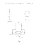
[0007] FIG. 1a shows an equivalent circuit for an inductor with a series resistance.
[0008] FIG. 1b shows an equivalent circuit for an inductor with a parallel resistance.
[0009] FIG. 2 is a circuit diagram for a conventional LC tank VCO.
[0010] FIG. 3 is a schematic illustration of a biasing circuit.
[0011] FIG. 4 is a schematic illustration of an LC tank VCO including the biasing circuit of FIG. 3.
[0012] FIG. 5 is a schematic illustration of a conventional ring-based VCO inverter stage.
[0013] FIG. 6 is a schematic illustration of a biasing circuit.
[0014] FIG. 7 is a schematic illustration of a ring-based VCO inverter stage including the biasing circuit of FIG. 6.
[0015] FIG. 8 is a block diagram of a ring-based VCO formed using a plurality of stages as shown in FIG. 7.
[0016] FIG. 9 is a block diagram of a phase-locked loop incorporating a ring-based VCO or a LC tank VCO as disclosed herein.
[0017] Embodiments of the present invention and their advantages are best understood by referring to the detailed description that follows. It should be appreciated that like reference numerals are used to identify like elements illustrated in one or more of the figures.
DETAILED DESCRIPTION
[0018] Reference will now be made in detail to one or more embodiments of the invention. While the invention will be described with respect to these embodiments, it should be understood that the invention is not limited to any particular embodiment. On the contrary, the invention includes alternatives, modifications, and equivalents as may come within the spirit and scope of the appended claims. Furthermore, in the following description, numerous specific details are set forth to provide a thorough understanding of the invention. The invention may be practiced without some or all of these specific details. In other instances, well-known structures and principles of operation have not been described in detail to avoid obscuring the invention.
[0019] Low noise and low power designs are disclosed herein for both LC tank VCOs as well as ring-based VCOs. The LC tank innovation will be addressed first
[0020] LC Tank VCO
[0021] In recent years monolithic inductors have appeared in CMOS and bipolar technologies, which made it possible to design integrated oscillators using an LC resonant circuit. A resonant "tank" is formed when an inductor L is placed in parallel with a capacitor C. The energy resonates within the tank at a frequency of ωres given by the following expression:
ω res = 1 LC . ##EQU00001##
At this resonant frequency the impedances of the capacitor and the inductor are equal and opposite, thereby giving an infinite impedance. However, in a real-world resonant tank, the inductors suffer from a series resistive component as shown by the equivalent circuit of FIG. 1(a). The series resistance of FIG. 1(a) can be transformed into an equivalent parallel resistance of FIG. 1(b), which lends itself to easier analysis and design. The equivalent circuit of FIG. 1(b) has the same reactance but has a resistance Rp that is Q2 times the series resistance Rs, where Q is the quality factor for the inductor. Both Q and the series resistance Rs have been measured and simulated extensively for integrated circuit inductors. Thus, the parallel resistance Rp for such inductors at the frequencies of interest is known to an accurate approximation. The parallel inductance Lp may be considered to be equal to the inductance L.
[0022] A conventional LC tank VCO is shown in FIG. 2. The parallel resistance for inductors Lp is not shown for illustration clarity. Two "LC tanks" are formed by the combination of the capacitances from a pair of varactors V1 and V2 and the parallel inductance Lp for a pair of inductors L. A differential pair of transistors M1 and M2 have their drains coupled to respective ones of the inductors L. A control voltage Vcontl controls the capacitance of varactors V1 and V2 so as to control the oscillation frequency. The drain voltage for M1 drives the gate of M2. Similarly, the drain voltage for M2 drives the gate of M1. Thus, as the drain voltage for M1 rises, the drain voltage for M2 falls because M2 is switched on. Similarly, as the drain voltage for M2 rises, the drain voltage for M1 falls because M1 is switched on. In this fashion, a tail current I conducted through a current source transistor M3 is switched between M1 and M2 responsive to oscillation of the LC tank VCO.
[0023] The oscillation condition for the LC tank VCO is given by the following expression:
(gm1,2Rp)2≧1,
where gm1,2 is the transconductance of either M1 and M2 (their transconductances being equal since they are a matched pair). If the startup condition is satisfied, the noise component at the resonant frequency are continually amplified by M1 and M2, thus leading to oscillation. If (gm1,2Rp)2≧1, then the oscillation amplitude grows until the loop gain drops at the peak, limiting the maximum amplitude.
[0024] The transconductance of the differential pair M1 and M2 thus plays a key role in determining the startup condition of LC tank voltage controlled oscillators. For any differential pair, the transconductance of M1 and M2 is proportional to that of M3 such that gm1=gm2=Agm2, where A is a proportionality constant and gm3 is the transconductance for M3. In particular, if M1, M2 and M3 all have the same widths and lengths, then the currents through M1 and M2 are half the current through M3 (at equilibrium). In such a case, gm1,2 equals gm3/sqrt(2), where sqrt represents the square root function. It follows that if the transconductance of M3 could be made proportional to 1/Rp, the transconductances of M1 and M2 would also become proportional to 1/Rp. The start up condition for oscillation would then depend only on the ratio of resistors and hence would become independent of temperature and process.
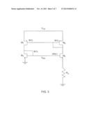
[0025] Turning now to FIG. 3, a supply-independent biasing circuit 300 is shown that achieves this advantageous biasing. Biasing circuit 300 includes a pair of PMOS transistors M6 and M7 in a current mirror relationship such that the drain and gate for transistor M6 as well as the gate for M7 have the same voltage. Since PMOS transistors M6 and M7 form a current mirror, their dimensions as defined through a width (W) and a length (L) ratio W/L are matched. The drain of M7 couples to a drain for an NMOS transistor M4 whose source couples to ground. M4 also has the same W/L ratio. The drain and gate of M4 are coupled together to force M4 into saturation responsive to a gate voltage VM4. The drain of M6 couples to a drain of another NMOS transistor M5 whose source couple to ground through a resistance Rp. In contrast to the other transistors, M5 has a W/L ratio that is a factor X times larger. But for this size difference, transistors M4 and M5 would also be in a current mirror relationship. It may be shown that the transconductance for M4 (denoted as gm4) equals (2/Rp)(1-1/sqrt(X)). The transconductance for M4 is thus equaling the desired proportionality to a resistance as discussed above with regard to current source transistor M3. Thus, if the dimensions for M3 are made to match those for M4 (same W/L ratio) and if M3 has the same biasing voltage (setting VISS of FIG. 2 equal to VM4 of FIG. 2), then the transconductance gm3 also equals (2/Rp)(1-1/sqrt(X)). As discussed previously, the transconductance gm1,2 equals Agm3. It can be seen that X must be larger than one or the transconductance become zero. For example, X can equal ten or any other suitable value larger than one.
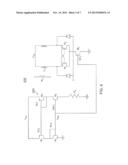
[0026] The startup condition of gm1,2Rp≧1 thus becomes 2A(1-1/sqrt(X))≧1. Such a startup condition depends only on the ratio of device widths, which is plainly independent of process corners, temperature, and supply voltage variations. FIG. 4 shows an LC tank VCO 400 that incorporates biasing circuit 300. The gate voltage VM4 is also the gate voltage for M3, which is matched to M4. In contrast, the bias voltage VISS shown for the conventional LC tank VCO of FIG. 2 is typically generated by a bandgap reference so as to achieve oscillation assuming a worst-case transconductance gm1,2. Such a worst-case biasing voltage wastes energy in that the tail current I is made larger than it needs to be should the transconductance gm1,2 be more optimal than the worst case that must be designed for. In contrast, VCO 400 is self-compensating and thus achieves low power operation.
[0027] VCO 400 also achieves low phase noise as well. In general, VCOs experience amplitude limiting and hence nonlinearity. This effect arises when odd-order nonlinearity in the amplitude leads to intermodulation between an injected noise component and the carrier. In order to account for the effect of noise due to real world nonlinearity, the well-known Leeson's equation for determining phase noise should be multiplied by a factor α, where α=gm1,2Rp is the actual small signal gain.
[0028] To ensure that oscillation starts, VCOs based on prior art technologies set α=gm1,2Rp≧1 for the worst case (usually hot and slow process corners). However, the value of a can be significantly larger for other corners compared to the worst case. Moreover, the magnitude of variations of Rp across process and temperature is not necessarily as much or in the same direction as the magnitude of variations of gm1,2). Therefore the phase noise of LC tank VCOs based on prior art technologies varies across process corners, temperatures, and supply voltage. In contrast, the value of a disclosed herein is self-compensating and constant. Hence the phase noise of LC tank VCOs as disclosed herein is the same across all process corners, temperatures and supply voltages.
Ring-Based VCOs
[0029] FIG. 5 shows a stage 500 of a ring-based VCO. Pfets P1 and P2 with threshold voltage of V.sub.th,P operate in the triode region, each acting as a variable resistor controlled by Vcntl. The on-resistance of P1 and P2 operating in deep triode is given by
RonP1,P2=1/(μp(W/L)Cox[VDD-Vcntl-|V.sub.th,p- |]2)
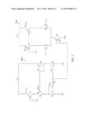
where μp is the hole mobility, W/L is the width to length ratio, and V.sub.th,p is the threshold voltage for P1 and P2. PFETS P1 and P2 thus act as voltage-controlled resistors. As Vcntl becomes more positive, the on-resistance of triode FETS P1 and P2 increases, thus increasing the time constant τ, which equals CL times RonP1,P2, where CL is the total capacitance from the output to ground. The oscillation frequency fosc is inversely proportional to the delay of the circuit, i.e., to τ. Thus the oscillation frequency can be controlled by varying Vcntl and is linearly proportional to this control voltage.
[0030] In stage 500, a differential pair of transistors NMOS transistors M1 and M2 steer a tail current sourced by a current source NMOS transistor M3 analogously as discussed with regard to the LC tank VCO of FIG. 2. The drain of M1 couples to the drain of P1. Similarly, the drain of M2 couples to the drain of P2. The startup condition is given by Equation (2) discussed above. Thus, if the transconductance of M1 and M2 can be made proportional to 1/RonP1,P2, the startup condition for a ring-based VCO becomes independent of process corner, temperature, and supply voltage variations.
[0031] FIG. 6 shows a biasing circuit 600 that achieves such a desirable result. PFETs M7 and M6 as well as NMOS transistors M4 and M5 are coupled together as discussed with regard to biasing circuit 300 of FIG. 3. However, the source of M5 for biasing circuit 600 couples to ground instead of a parallel resistance of the inductor. The source of M7 couples to the power supply voltage through a triode-mode PFET P3 that is matched to PFETs P1 and P2 of VCO stage 500. The resistance of P3 is denoted as Ron,P3 and is given the following expression:
Ron,P3=μpCox(Wp/Lp)(Vdd-Vcntl)
[0032] where μp is the hole mobility, Cox is the oxide capacitance, Wp is the transistor width, and Lp is the transistor length. This resistance then controls the current through M7 and thus through M6 because of the current mirror relationship. It follows that the current I through M6 is given by
I=(2/μpCox(W/L)*(1/Ron,P3)2*(1-1/sqrt(X))2
[0033] The transconductance for M6 is denoted as gm6 and given by the following expression:
gm6=sqrt(2μpCox(W/L)I)=(2/Ron,P3)(1-1/sqrt(X))
[0034] The transconductance of M4 (gm4) is related to that of M6 by
Gm4=sqrt(μn/μp)gm6
where μn is the electron mobility in M4. Thus gm4 is given by
gm4=sqrt(μn/μp)(2/Ron,P3)(1-1/sqrt(X))
[0035] This transconductance setting can be exploited as shown for VCO stage 700 of FIG. 7. Rather than use a bandgap reference voltage to bias current source transistor M3 as is conventional, the gate voltage VM4 from M4 in biasing circuit 600 drives the gate of M3. This is quite advantageous in that the M3 is matched to M4 such that the transconductance for M3 (gm3) is equal to gm4. As discussed with regard to the LC tank VCO, the transconductance for the differential pair of transistors M1 and M2 (denoted as gm1,2) equals gm3 times a proportionality constant A. It follows that the startup condition for a ring-based VCO utilizing a plurality of stages 700 becomes
gm1,2RonP1,P2=2A sqrt(μn/μp)(RonP1,P2/Ron,P3)(1-1/sqrt(X)).gtore- q.1
[0036] If P1, P2, and P3 are all matched, then RonP1,P2 equals Ron,P3. The startup condition thus becomes
gm1,2RonP1,P2=2A sqrt(μn/μp)(1-1/sqrt(X))≧1
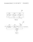
This shows that the startup condition depends only on the ratio of device widths and the ratio of the device mobilities. Because such ratios are independent of process corner, temperature, and power supply noise, so is the startup condition. A resulting ring-based VCO 800 that incorporates stage 700 is shown in FIG. 8. Biasing circuit 600 need not be duplicated for each stage such that a single biasing circuit can bias all the inverter stages.
[0037] Regardless of whether an LC tank or a ring-based VCO is constructed as discussed herein, the resulting VCO may be advantageously incorporated into many circuits. The self-compensating oscillation and startup properties of VCO 800 have many applications. For example, VCO 800 (or 300) may be incorporated into a phase-locked loop (PLL) 900 as shown in FIG. 9 that includes a phase detector 910, a loop filter 915, and a loop divider 920. VCO 800 responds to the control voltage Vcontrol as discussed above to control its output frequency. Advantageously, this output signal frequency will not depend on the particular semiconductor process corner used to manufacture the integrated circuit forming VCO 800. Moreover, the startup conditions will not depend on operating temperature changes or process variations.
[0038] It will be appreciated that the techniques and concepts discussed herein are not limited to the specific disclosed embodiments but instead may be changed or modified. The appended claims encompass all such changes and modifications as fall within the true spirit and scope of this invention.
User Contributions:
Comment about this patent or add new information about this topic:
Images included with this patent application:
 |  |
 |  |
 |  |
 |  |
| Similar patent applications: | |
| Date | Title |
|---|---|
| 2010-11-04 | Wideband voltage translators |
| 2014-01-30 | Power on reset device and power on reset method |
| 2009-06-25 | Low vt dependency rc oscillator |
| 2014-01-23 | Injection-locked-type frequency-locked oscillator |
| 2014-01-30 | Bypass for on-chip voltage regulator |
| New patent applications in this class: | |
| Date | Title |
|---|---|
| 2016-09-01 | Phase locked loop with sub-harmonic locking prevention functionality |
| 2016-06-30 | Method and apparatus to suppress digital noise spurs using multi-stage clock dithering |
| 2016-06-02 | Time-to-digital converter using stochastic phase interpolation |
| 2016-03-17 | Systems and methods for frequency domain calibration and characterization |
| 2016-03-03 | Foreground and background bandwidth calibration techniques for phase-locked loops |
| New patent applications from these inventors: | |
| Date | Title |
|---|---|
| 2013-08-29 | Voltage-controlled oscillator with amplitude and frequency independent of process variations and temperature |
| 2013-08-01 | Low-power voltage-controlled oscillator |
| 2013-06-27 | Tunable transconductance-capacitance filter with coefficients independent of variations in process corner, temperature, and input supply voltage |
| Top Inventors for class "Miscellaneous active electrical nonlinear devices, circuits, and systems" | |
| Rank | Inventor's name |
|---|---|
| 1 | Yantao Ma |
| 2 | Feng Lin |
| 3 | Ming-Chieh Huang |
| 4 | Yong-Ju Kim |
| 5 | Chan-Hong Chern |