Patent application title: MODELING TECHNIQUE FOR RESISTIVE RANDOM ACCESS MEMORY (RRAM) CELLS
Inventors:
Wei Lu (Ann Arbor, MI, US)
Wei Lu (Ann Arbor, MI, US)
Assignees:
Crossbar, Inc.
IPC8 Class: AG06F1750FI
USPC Class:
703 14
Class name: Data processing: structural design, modeling, simulation, and emulation simulating electronic device or electrical system circuit simulation
Publication date: 2012-06-28
Patent application number: 20120166169
Abstract:
Accurate simulation of two-terminal resistive random access memory (RRAM)
behavior is accomplished by solving equations including state variables
for filament length growth, filament width growth, and temperature. Such
simulations are often run in a SPICE environment. Highly accurate models
simulate the dynamic nature of filament propagation and multiple
resistive states by using a sub-circuit to represent an RRAM cell. In the
sub-circuit, voltages on floating nodes control current output while the
voltage dropped across the sub-circuit controls growth and temperature
characteristics. Properly executed, such a sub-circuit can accurately
model filament growth at all phases of conductance including dynamic
switching and a plurality of resistive states.Claims:
1. A computer-implemented method for modeling a circuit including a
resistive random access memory (RRAM) cell, the method comprising:
providing a circuit including at least one RRAM cell in a display area of
a computer system, the RRAM cell being associated with a first internal
state variable; calling a sub-circuit module that represents the RRAM
cell and has a first component that corresponds to a formula for solving
the first internal state variable; modeling a characteristic of the
circuit using the sub-circuit module; adjusting the circuit using a
result of the modeling step; and storing the adjusted circuit in a
storage location associated with the computer system.
2. The method of claim 1, wherein the first internal state variable is represented by a simulated electrical component.
3. The method of claim 2, wherein the electrical component is a current source, voltage source, capacitor, inductor, resistor, transistor, diode, or a combination thereof.
4. The method of claim 1, wherein the formula includes a formula representing dynamic length growth of a filament in the RRAM.
5. The method of claim 4, further comprising a formula representing dynamic width growth of a filament in the RRAM.
6. The method of claim 1, wherein the modeling includes hysteretic growth behavior representing separate length growth and width growth phases.
7. The method of claim 5, wherein the width characteristic is modeled by simulating a plurality of filaments.
8. The method of claim 5, wherein the width characteristic is modeled by varying a lateral dimension of a filament.
9. The method of claim 4, wherein the length growth characteristic is represented by the equation: l t = d τ 0 exp ( - U a V thermal ) ( sinh ( V ex V 0 ) ) . ##EQU00008##
10. The method of claim 1, wherein the width growth is represented by the equation (equation).
11. The method of claim 1, wherein the temperature characteristic node is further configured to influence the values of the length growth node and the width growth node.
12. The method of claim 1, wherein the RRAM cell is configured to register more than binary final resistance states.
13. The method of claim 1, wherein the RRAM cell is associated with a second internal state variable, the first internal variable relating to a length growth of a filament of the RRAM and the second internal variable relating to a width growth of the filament of the RRAM.
14. The method of claim 1, wherein the simulation is conducted in a Simulation Program with Integrated Circuit Emphasis (SPICE) environment.
Description:
CROSS-REFERENCES TO RELATED APPLICATIONS
[0001] This application claims priority from provisional U.S. Provisional Application No. 61/427,741, filed Dec. 28, 2010, entitled "Modeling Technique for Resistive Random Access Memory Cells," the entire disclosure of which, including all attachments and appendices, are incorporated by reference in their entirety for all purposes.
BACKGROUND OF THE INVENTION
[0002] The present invention relates to simulation of Resistive Random-Access Memory (RRAM) or other two-terminal resistive devices with hysteresis. Such devices are also sometimes termed memristors.
[0003] RRAM is a type of resistive memory that has generated significant interest as a potential candidate for ultra-high density non-volatile information storage. Fabrication costs of RRAM designs are substantial, so considerable savings can be realized by optimizing design by modeling RRAM in a simulated environment. As RRAM technology becomes available to circuit designers, there will be an increasing need for accurate modeling and simulation tools.
[0004] A working principle of RRAM devices is the formation of a conductive path governed by a filamentary process. In an exemplary device, in the presence of an applied electric field, silver ions migrate through an amorphous silicon solid electrolyte to form a conductive filament along which electrons can travel. As current passes through the device, Joule heating raises the device temperature, which affects filament growth. Filament growth exists in at least two different forms, including extension of length between electrodes and an increase in width, both of which have an effect on the electrical properties of an RRAM cell.
[0005] Two-terminal RRAM has several unusual properties. For example, under the application of a bias voltage, the activation energy of a silver ion varies with distance as it moves from a source electrode to a destination electrode, and the amplitude of subsequent energy peaks decreases with respect to distance as the ion passes through imperfections in a semiconductor matrix. When a two-terminal RRAM cell is coupled to a resistor in series, variance of the resistance value of the resistor can affect the final resistance of the RRAM cell, thereby allowing the cell to retain additional data.
[0006] Current simulation models typically utilize a fixed threshold voltage to activate an RRAM write cycle. Such models assume that a single set voltage will result in changing a resistance value from an ON state to an OFF state, or vice versa. However, the threshold voltage is dynamic in an actual two-terminal RRAM device. Using a fixed voltage fails to capture some of its unique properties, and otherwise results in an inaccurate simulation.
[0007] Current simulation models typically utilize a fixed switching time to activate an RRAM write cycle. However, the switching time is dynamic in an actual two-terminal RRAM device and varies with respect to voltage. Using a fixed switching time fails to capture some of its unique properties, and otherwise results in an inaccurate simulation.
[0008] There is a need for an accurate simulation model that accurately models the dynamic characteristics of a two-terminal RRAM cell. Although equations have been established to represent some aspects of memory cell performance, existing simulation models are not capable of simultaneously accounting for the variables of ion growth and current in the greater context of a circuit. An RRAM simulation method and system capable of resolving the dynamic relationship between state variables and properties in an RRAM cell would aid the task of incorporating these important new technologies into circuit designs, and help bring the use of RRAM devices closer to realization.
BRIEF SUMMARY OF THE INVENTION
[0009] The present invention relates to simulation of RRAM behavior.
[0010] In an embodiment, a computer-implemented method for modeling a circuit includes a resistive random access memory (RRAM) cell. The method includes providing a circuit including at least one RRAM cell in a display area of a computer system, the RRAM cell being associated with a first internal state variable; calling a sub-circuit module that represents the RRAM cell and has a first component that corresponds to a formula for solving the first internal state variable; modeling a characteristic of the circuit using the sub-circuit module; adjusting the circuit using a result of the modeling step; and storing the adjusted circuit in a storage location associated with the computer system.
[0011] The details of one or more embodiments are set forth in the accompanying drawings and the description below. Other features, objects, and advantages will be apparent from the description and drawings, and from the claims.
BRIEF DESCRIPTION OF THE DRAWINGS
[0012] Exemplary embodiments will hereinafter be described in conjunction with the appended drawings, wherein like designations denote like elements, and wherein:
[0013] FIG. 1 illustrates a computer system according to an embodiment of the present invention;
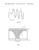
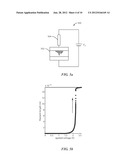
[0014] FIG. 2a illustrates a length growth phase of a two-terminal RRAM cell;
[0015] FIG. 2b illustrates the activation energy experienced by a silver ion as it moves through a silicon matrix towards an electrode in a two-terminal RRAM cell;
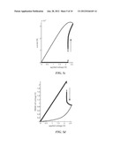
[0016] FIG. 3 illustrates a width growth phase of a two-terminal RRAM cell;
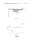
[0017] FIG. 4 illustrates hysteretic switching behavior of a two-terminal RRAM cell;
[0018] FIG. 5a illustrates a simple circuit according to an embodiment of the present invention;
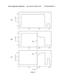
[0019] FIG. 5b illustrates filament length as a function of voltage where the line of large dots shows an increase in filament length as voltage increases to 2.5V, and the line of small dots shows the filament length as voltage decreases back to zero in a two-terminal RRAM cell;
[0020] FIG. 5c illustrates current as a function of voltage in a voltage sweep where the line of large dots represents current as voltage increases to 2.5V, and the line of small dots shows the current as voltage decreases back to zero in a two-terminal RRAM cell;
[0021] FIG. 5d illustrates voltage as a function of applied voltage in a voltage sweep where the line of large dots represents voltage as the applied voltage increases to 2.5V, and the line of small dots shows voltage as the applied voltage decreases back to zero in a two-terminal RRAM cell;
[0022] FIG. 5e illustrates the temperature of a two-terminal RRAM cell with respect to time when a voltage is applied according to FIG. 5f;
[0023] FIG. 5f illustrates a voltage curve applied to a two-terminal RRAM cell;
[0024] FIG. 6a illustrates the layout of a sub-circuit corresponding to an RRAM cell.
[0025] FIG. 6b illustrates the layout of a sub-circuit using components to hold state variables representing RRAM behavior.
[0026] FIG. 7a illustrates a final resistance of a two-terminal RRAM cell after applying 4.75V for 50 nanoseconds through a variable resistor Rs;
[0027] FIG. 7b illustrates switching time of a two-terminal RRAM cell with respect to voltage;
[0028] FIG. 8a illustrates a voltage curve with respect to time applied to a two-terminal RRAM cell and a series resistor, with a programming pulse followed by a read pulse;
[0029] FIGS. 8b and 8c illustrate current and voltage with respect to time in a two-terminal RRAM cell when the voltage pulses in FIG. 8a are applied, with a switching event at 36 nanoseconds and Vcell is the RRAM cell voltage; and
[0030] FIG. 9 illustrates a flowchart of a method for simulating an RRAM cell according to an embodiment of the present invention.
DETAILED DESCRIPTION OF THE INVENTION
[0031] The present invention relates to simulation of Resistive Random-Access Memory (RRAM).
[0032] The embodiments presented herein are described in context with amorphous silicon based RRAM cells. However, the invention is not limited to these embodiments, but can be practiced with other types of RRAM devices, including RRAMs based on metal oxide, chalcogenide based and organic materials.
[0033] The `Simulation Program with Integrated Circuit Emphasis` (SPICE) is one of the most widely used simulation engines for device modeling and provides and extensible framework for the addition of new components. Although RRAM modeling techniques and certain embodiments are described herein in connection with SPICE, the framework and the modeling techniques may be used with circuit simulation software programs other than SPICE.
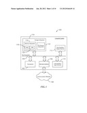
[0034] FIG. 1 illustrates a simplified block diagram of an exemplary computer system 100 according to an embodiment of the present invention. Computer system 100 typically includes at least one processor 102, which communicates with a number of peripheral devices via bus subsystem 104. These peripheral devices typically include a storage subsystem 114, user interface input devices 110, and a network interface subsystem 106. The input and output devices allow user interaction with computer system 100. It should be apparent that the user may be a human user, a device, a process, another computer, and the like. Network interface subsystem 106 provides an interface to outside networks.
[0035] User interface input devices 110 may include a keyboard, pointing devices such as a mouse, trackball, touchpad, or graphics tablet, a scanner, a touchscreen incorporated into the display, audio input devices such as voice recognition systems, microphones, and other types of input devices. In general, use of the term "input device" is intended to include all possible types of devices and ways to input information into computer system 100 or onto communication network 108.
[0036] User interface output devices 112 may include a display subsystem, a printer, a fax machine, or non-visual displays such as audio output devices. The display subsystem may be a cathode ray tube (CRT), a flat-panel device such as a liquid crystal display (LCD), or a projection device. The display subsystem may also provide non-visual display such as via audio output devices. In general, use of the term "output device" is intended to include all possible types of devices and ways to output information from computer system 100 to a user or to another machine or computer system.
[0037] Storage subsystem 114 stores the basic programming and data constructs that provide the functionality of the computer system. For example, the various modules implementing the functionality of the present invention may be stored in storage subsystem 114. These software modules are generally executed by processor(s) 102. In a distributed environment, the software modules may be stored on a plurality of computer systems and executed by processors of the plurality of computer systems. Storage subsystem 114 also provides a repository for storing the various databases storing information according to the present invention. Storage subsystem 114 typically comprises memory subsystem 116 and file storage subsystem 122.
[0038] Memory subsystem 116 typically includes a number of memories including a main random access memory (RAM) 120 for storage of instructions and data during program execution and a read only memory (ROM) 118 in which fixed instructions are stored. File storage subsystem 122 provides persistent (non-volatile) storage for program and data files, and may include a hard disk drive, a floppy disk drive along with associated removable media, a Compact Digital Read Only Memory (CD-ROM) drive, an optical drive, removable media cartridges, and other like storage media. One or more of the drives may be located at remote locations on other connected computers at another site on communication network 108. Information stored according to the teachings of the present invention may also be stored by file storage subsystem 122.
[0039] Bus subsystem 104 provides a mechanism for letting the various components and subsystems of computer system 100 communicate with each other as intended. The various subsystems and components of computer system 100 need not be at the same physical location but may be distributed at various locations within a distributed network. Although bus subsystem 104 is shown schematically as a single bus, alternative embodiments of the bus subsystem may utilize multiple busses.
[0040] Computer system 100 itself can be of varying types including a personal computer, a portable computer, a workstation, a computer terminal, a network computer, a mainframe, or any other data processing system. Due to the ever-changing nature of computers and networks, the description of computer system 100 depicted in FIG. 1 is intended only as a specific example for purposes of illustrating the preferred embodiment of the computer system. Many other configurations of a computer system are possible having more or fewer components than the computer system depicted in FIG. 1. Client computer systems and server computer systems generally have the same configuration as shown in FIG. 1, with the server systems generally having more storage capacity and computing power than the client systems.
[0041] The electrical behavior of RRAM is complex, and in the case of two-terminal RRAM, may take place in multiple discrete phases during a write cycle. These include a length growth phase and a width growth phase. These phases have distinct characteristics which must be dealt with separately in order to accurately model RRAM behavior.
[0042] The first stage of filament growth in an RRAM cell 200 is shown in FIG. 2a. In the first stage of filament growth, the length `l` of a filament 202, which is the distance between filament front 206 and top electrode 204, grows as ions from the top electrode 204 are oxidized and migrate along the applied electric field towards the bottom electrode 208. The distance between top electrode 204 and bottom electrode 208 is represented as `h`. In the absence of an applied voltage, the velocity of the filament front can be derived as follows:
l t = d τ 0 ( exp ( - U a V Therm ) - exp ( - U a V Therm ) ) = 0 ##EQU00001##
Where Vtherm=kT/q and d is the hopping site distance, or distance between impurities, τ0 is the material-dependent ion hop attempt frequency, Ua is the activation energy, k is Boltzmann's constant in J/K, T is the temperature in Kelvin, q is the charge on an electron, and l is the filament length as shown in FIG. 2a.
[0043] As a silver ion moves from one impurity in the silicon matrix to another under an applied voltage V, it experiences changes in the potential energy barrier. The potential energy decreases with respect to distance according to the equation Vd/2(h-l). This behavior is illustrated in FIG. 2b, in which the solid line represents the actual potential energy barrier experienced by a silver ion. The distance between peaks is the hopping site distance d, and the difference between the dotted line, which represents equilibrium behavior, and the solid line is caused by the decreasing potential energy, where applying a voltage V reduces the barrier height. Thus, Equation 1 for deriving filament length with respect to time is:
[ Eq . 1 ] l t = d τ 0 ( exp ( - U a + V d 2 V Therm ) - exp ( - U a - V d 2 V Therm ) ) = d τ 0 exp ( - U a V Therm ) ( exp ( V d 2 V Therm ) - exp ( V d 2 V Therm ) ) ( 1 ) ##EQU00002##
where Vd is the voltage dropped between each hopping site.
V d = Ed = V h - l d ##EQU00003##
where h is distance between electrodes as shown in FIG. 2. Letting
V 0 = 2 V thermal ( h - 1 ) d ##EQU00004##
leads to simplified Equation 2, which is an exemplary embodiment of an equation for modeling filament length growth in an RRAM cell. Equation 2 is:
[ Eq . 2 ] l t = d τ 0 exp ( - U a V thermal ) ( exp ( V V 0 ) - exp ( - V V 0 ) ) = d τ 0 exp ( - U a V thermal ) ( sinh ( V V 0 ) ) ( 2 ) ##EQU00005##
[0044] After the filament length/has reached a value such that the filament essentially touches the bottom electrode (e.g. characterized by the conductance being equal to the conductance quantum (7:748×10-5 S), or the spacing between the filament front 206 and the bottom electrode 208 being equal to the lattice spacing of the metal ion), vertical growth halts and the filament enters the second growth stage, characterized by the expansion of its width as shown in FIG. 4. The growth of the filament's diameter or width or area can be modeled as the addition of conductive filaments in parallel with the first. Thus, Equation 2 can be used when modeling the width growth as well. During width growth, the term h-l remains constant, so the second stage of growth is a simpler function of voltage.
[0045] During the first growth phase, the width variable remains equal to zero, and so the RRAM cell current is determined solely by the tunneling junction formed between the conductive filament 202 and the bottom electrode 208. Different models, including direct tunneling, trap-assisted tunneling, Frenkel-Poole conduction, and linear or non-linear resistor models, can be used to describe the current between the filament 202 and the bottom electrode 208. In an embodiment, the I-V can be calculated using a tunneling model according to the following Equation 3:
[Eq. 3]
ITunneling=sin VAreaJ0(Pqexp(-A {square root over (Pq)}exp(Pq+q|V|)exp(-A {square root over (Pq+q|V|)})) (3)
where
J 0 = q 2 π h 0 s 2 ##EQU00006## A = 4 π x 2 m h 0 ##EQU00006.2## s = h - l ##EQU00006.3##
and Pq is the average barrier height, h is the distance between electrodes, l is the length of the conductive filament, q is the charge on an electron, Area is the area of the end of a filament, h0 is Plank's constant, and m is the mass of an electron.
[0046] Because tunneling current is exponentially dependent on barrier thickness, a dramatic increase in cell conductance occurs as the filament approaches the bottom electrode 208. It is during this phase that the cell is qualitatively said to have switched in a digital sense to the `ON` state.
[0047] When a cell enters the width growth phase, further increases in current density are the result of areal expansion of the filament. The expansion can be described either in terms of increasing the number of filaments, or as increasing the cross-sectional area of a single filament. When the filament makes Ohmic contacts with the electrodes, the current is then determined as a function of width by Equation 4:
[Eq. 4]
Iwidth=VwidthG0 (4)
where the variable width represents a number of filaments, and G0 is the conductance through a single filament, which is normally constant for a given material. The total current consists of the sum of the two conduction regimes (Equations 3 and 4), as shown in Equation 5:
[Eq. 5]
I=ITunneling+IWidth (5)
[0048] In another case the current due to width growth can be described by Equation 6 which includes the Schottky term (1st term) and the tunneling term (2nd term):
[Eq. 6]
Iwidth=(1-w)α[1-exp(-βV)]+wγ sin h(δV) (6)
The two conduction channels are in parallel and their relative weight is determined by the internal state variable w, which is the normalized area index representing the conductive region, i.e. w=0 indicates fully Schottky-dominated conduction, while w=1 indicates fully tunneling-dominated conduction. α, β, γ, δ, η1, and η2 are all positive-valued parameters determined by material properties such as the barrier height for a Schottky barrier and for tunneling, the depletion width in the Schottky barrier region, the effective tunneling distance in the conducting region, and interface effects. In practice they can be treated as fitting parameters and are independent of w.
[0049] It is possible that the programming process can be dominated by either length growth or width growth; in that case, I will be dominated by ITunnel or Iwidth in Equation 5.
[0050] The following Equations 7 is useful for describing the width propagation phase of RRAM cell activity.
[ Eq . 7 ] w t = λ [ exp ( η 1 V ) - exp ( - η 2 V ) ] ( 7 ) ##EQU00007##
Equation 7 describes the rate of change of the state variable representing width with respect to the applied voltage. It originates from Equation 3 but is no longer explicitly dependent on the state variables/or w since the existing conductive regions do not affect the formation of new conductive regions. The expression is further chosen such that (dw/dt) can be different at positive and negative biases (η1≠η2) to account for potential differences in the activation energies for forward and backward ion hopping, e.g. in the presence of a build-in field. Having asymmetric activation energies (η1≠η2) however is not essential in modeling. When η1≠η2 Equation 7 becomes a simpler form of Sin h(ηV).
[0051] The growth and retraction of a conductive filament through a length growth and width growth phase leads to hysteretic behavior in an RRAM cell that can be accurately modeled using the above equations. Representative hysteretic behavior is shown by the I-V curve in FIG. 4.
[0052] As switching occurs, current passes through the device, and thus, power is dissipated within the body of the cell, thereby raising its temperature. Because both tunneling current and filament growth are positively correlated with device temperature, a positive feedback mechanism accelerates the growth of the filament and enhances current output.
[0053] Despite the rise in temperature and corresponding barrier height reduction, filament growth is halted when the electric field through the device diminishes. Nevertheless, temperature effects can play an important role in determining the final resistance value after switching. An embodiment in a SPICE environment allows for the incorporation of temperature effects through the `temp_ coeff ` parameter, which serves as the heat capacity of the device in units K/W.
[0054] FIG. 5a shows a circuit 500 used in a simulation program, including a RRAM device 502 connected in series with a resistor 504 and voltage source Va. In various embodiments, resistor 502 can be replaced with current-compliance, a diode, or a transistor. FIGS. 5b to 5d show the effects of a voltage sweep performed on RRAM device 502 in circuit 500.
[0055] As a filament grows with applied voltage, as shown in FIG. 5b, the current through the device sharply increases due to the non-linear effects described in Equations 2 and 3 as shown in FIG. 5c. In the meantime, a voltage divider effect between the device and the series resistor reduces the voltage applied across the cell, as shown in FIG. 5d. The reduced electric field within the device in turn retards further filament growth. FIG. 5e shows a temperature profile over time in a cell according to the applied voltage over time shown in FIG. 5f.
[0056] Various embodiments can incorporate various physics models in a simulation within the scope and spirit of the invention. In an exemplary embodiment, SPICE code using Equation 2 and Equation 5 for an RRAM component was constructed, and is featured in Table 1 below. Because most SPICE simulation environments cannot handle equations such as Eq. 3 directly and do not allow for arbitrary internal mutable variables, floating node capacitors are used to store the state variables required by the model. Thus, voltage or other electrical properties act as a proxy for physical state variables. In some embodiments, by using the SPICE `.ic` directive, initial conditions can be imposed on the state variables. This allows the user to begin a simulation with cells in the `ON,` or even intermediate states.
TABLE-US-00001 TABLE 1 SPICE code listing for a two-terminal RRAM device *Parameters: *to is hopping attempt frequency *area is device area *d is site hopping distance *w is device length *Ua is ion barrier height *P is electron barrier height .subckt memristor 3 1 params: + to=4e12 area=1e-16 d=1-9 Ua=0.87 w=2.29e-9 P=.31 Rfil=100 *Notes: ************************************************************ *In any function where k is a parameter, k is simply a dummy variable, always called with 0 and not *used in the function. A function was simply used for clarity. ************************************************************ .param k=1.38e-23 ;Boltzman's Constant .param echarge=1.6021e-19 ;Charge on electron .param temp_coeff=3e5 ;Specific Heat of Silver .param th_conduct=0 ; .param plank = {6.62606e-34} ;Plank's Constant .param Pq={P*echarge} ;Electron Barrier Height .param m={0.09*9.109e-31} ;effective mass of an electron .param lamda=0.03 a1=2.1 a2=2.3 .param nnor=1e-9 .param cpac={1} .func T(z) 300 + temp_coeff*V(1,3)*I(Rmet) .func Vthermal(z) {k*T(0)/echarge} Rmet 1 2 {Rfil} *Current Output: .func A(z) {4*Pi*(w-cpac*V(length))*sqrt(2*m)/plank} .func Jo(z) {echarge/(2*Pi*plank*(w-cpac*V(length))**2)} .func J_tun(z) {sgn(V(2,3))*area*Jo(0)*(Pq*exp(-(0)*sqrt(Pq))- (Pq+echarge*abs(V(2,3)))*exp(-A(0)*sqrt (Pq+echarge*abs(V(2,3)))))} Bw 2 3 I=J_tun (0) + V(2,3)*(V(width))*(77e-6) *State variables: Clength length 0 1 Cwidth width 0 1 Ctemp temp 0 1 *Initial Conditions: .ic V(length) = .1e-12 .ic V(width) = 0 .ic V(temp) = 300 *Supplementary Functions: .func Vo(z) 2*Vthermal(0)*(w-cpac*V(length))/d .func ion_flow(z) { d*to*exp(- Ua/Vthermal(0))*(exp(V(2,3)/Vo(0))-exp(-V(2,3)/Vo(0))) } .func prev_underfloor(z) {u( sgn(cpac*V(length)-1e-12) + sgn(ion_flow(0)) + 1 ) } .func single_growth(z) {u(77e-6 - J_tun(0)/V(2,3))*(V(2,3)>=0) + (V(2,3)<0)*(V(width)<=0)} *State Variable Derivatives: Blength 0 length I=single_growth(0)*prev_underflow(0) *ion_flow(0) Bwidth 0 width I=(1-single_growth(0))*ion_flow(0)/V(length) Btemp 0 temp I=temp_coeff*V(1,3)*I(Rmet) .ends memristor
[0057] FIGS. 6a and 6b illustrate the layout of sub-circuits corresponding to the code in Table 1. The code can be thought of as having two parts. The first part is described by earlier sections of code including parameter definitions and functions through the line "*State variables." This portion of the code corresponds to the circuit illustrated in FIG. 6a. The circuit has three node locations 602, 604, and 606, corresponding to node 1, node 2, and node 3, respectively.
[0058] The sub-circuit 600 in FIG. 6a correlates to an actual RRAM cell, such as the cell represented in FIG. 2. Conceptually, node location 602 in FIG. 6a corresponds to top electrode 204, node location 604 corresponds to the filament front 206, and node 606 corresponds to bottom electrode 208. Resistor 608, located between node 602 and node 604, corresponds to the "Rmet" resistor in the Table 1 code, which represents the fixed parasitic resistance inside an RRAM cell. Variable resistor 610 represents the active region, or switching region, of an RRAM cell. Current is solved for this region of a cell using the "Bw" function in Table 1, which corresponds to Equation 5, and is a function of Vlength, V\width, input voltage, and temperature.
[0059] Portions of the code in Table 1 beginning with the term "*State variables" and extending to the end of Table 1 correspond to the sub-circuit 612 shown in FIG. 6b. Sub-circuit 612 comprises three nodes 614, 616, and 618, corresponding to nodes "length," "width," and "temp" in Table 1, respectively. A fourth node 620, node 0, is located at ground. Similarly, the circuit has three capacitors 622, 624, and 626, and three current sources 628, 630, and 632, one for each of the state variables representing length, width, and temperature. The capacitors are represented by Clength, Cnum, and Ctemp in Table 1, while the current sources are represented by Blength, Bwidth, and Btemp. In this embodiment, SPICE treats the internal state variables representing physical characteristics as voltages.
[0060] Although the code in Table 1 shows a capacitor Ctemp, it is not necessary to have a capacitor for temperature in order to run a simulation using the Table in some embodiments. The simulation can be performed using components other than capacitors to perform derivative functions. In other embodiments, the components may include a current or voltage source, inductor, resistor, transistor, diode, or a combination thereof. In the embodiment in Table 1, the voltages on the floating nodes control the filament (e.g. length and width) growth while the voltage dropped across the device controls the current output and temperature characteristics. Growth of length and width is accelerated by elevated temperatures.
[0061] Because the filament growth is exponentially dependent on the applied electric field, reducing the voltage across the device has a large impact on the derivative of the conductance. Using a series resistor, the filament growth can be controllably stopped at a specific conductance determined by the series-resistor, a consequence of which is the ability to reliably store more than two values of data in a cell.
[0062] In an embodiment according to circuit 500 in FIG. 5, when the RRAM device 502 is in the `OFF,` or high resistance state, nearly all of the voltage is dropped across the cell. As the filament grows, however, the resistance of the cell drops and a voltage divider is formed effect between the resistor 504 and the RRAM device 502 due to the series configuration. This has the effect of reducing the electric field within the solid electrolyte, which corresponds to much slower filament growth. The negative feedback provided by the voltage divider dampens growth exponentially with further increases in cell conductance until the voltage drop across the cells drops to the point that growth is imperceptible and the cell settles at a final resistance. This happens very quickly during the filament formation process.
[0063] FIG. 7a shows how the final resistance state is controlled by the use of resistors of various values. Thus, by controlling the series resistance using, for example, a series of resistors, a diode, a MOS selector, or different current compliance, multilevel resistance values can be achieved. This enables more than two values of data to be stored in each RRAM cell, thereby increasing data density with minimal increase in device footprint for controlling resistance. FIG. 7a shows the final resistance state after applying 4.75V for 50 nanoseconds through a variable resistor at various resistor values.
[0064] Because of the rapidity with which the device can change state, the RRAM simulation provided herein is particularly useful for capturing switching dynamics which may be hard to obtain using other, simpler simulations. In particular, the switching speed is not a constant for a given RRAM device, but rather is a sensitive function of the applied bias. For example, by examining Equation 2, we see that the switching delay, τ, is an exponential function of the voltage applied across the device. FIG. 7b shows the results of a model prediction, represented as a line, plotted against actual measured data, which is plotted as individual data points. FIG. 7b demonstrates that the SPICE model's predicted switching times fit the switching times reported experimentally. The SPICE simulation of this embodiment shows that τ is not dependent on the series resistance value.
[0065] The results output by the SPICE-based embodiment described above are consistent with the notion that the ion migration in two-terminal RRAM devices depends on the applied electric field. When an RRAM cell is in the `OFF` state, its resistance is orders of magnitude larger than any series resistor normally used in the circuit, so nearly all of the voltage is dropped across the device, causing it to switch.
[0066] FIG. 8 shows a typical write-read sequence in an RRAM cell using programming and read pulses. The switching event 802, represented by a dotted line, is defined qualitatively as a substantial rise in current with a corresponding reduction in the voltage dropped across the device. The switching event 802 occurs at 36 ns. After programming, the device is probed using a voltage pulse with a magnitude much smaller (1 volt in this case) than that used for programming. Using the current through the circuit and the voltage dropped across the RRAM cell, a final resistance value can be calculated at a given read voltage.
[0067] Following this write-read procedure, the final cell resistance values were found while varying the external series resistor 504. The final resistance state varies linearly for series resistance values below 1M, with superlinear dependence above. The nonlinear dependence beyond 1M can be attributed to the elongation of a switching event, such that the device will not have fully switched when a very high series resistance is used.
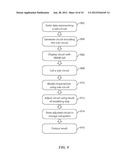
[0068] A method for implementing an RRAM simulation according to an embodiment will be now described with respect to FIG. 9. Although the embodiment is described as a simulation run in a SPICE environment, similar methods can be used in other simulation environments without departing from the scope and spirit of the invention.
[0069] A simulation can be conducted in SPICE software, or other electronic simulation software that accepts programmable data to model the performance of components. A user enters data in step 902, which includes data representing the electrical behavior of an RRAM cell. To accurately model two-terminal RRAM, the data should include at least an equation representing filament length growth. In an exemplary embodiment, the length growth equation is represented by Equation 2. Various embodiments can include various equations representing RRAM cell behavior, depending on the nature of the simulation and the desired level of accuracy. A highly accurate simulation can be made using Equation 2 to represent a length growth characteristic, Equation 7 to represent width growth, Equation 3 for tunneling current, equation 4 for areal expansion current, and a function such as the "temp_coeff" function in SPICE to represent thermal characteristics. An example of user data configured for SPICE is found in Table 1 above.
[0070] The data entry step 902 may include data that assigns equations to represent electrical components to build a sub-circuit. The specific components may be selected according to a component's ability to accept the equations, such as the derivative with respect to time in Equation 3. For example, the data in Table 1 uses floating capacitor nodes to store internal state variables. In other embodiments, components including a current source, voltage source, capacitor, inductor, resistor, transistor, or diode, or a combination of these components or their equivalents, can be used to store state variables.
[0071] The data may include initial conditions of variables in the simulated RRAM module, including conditions of filament length, filament width, and device temperature. In the embodiment shown in Table 1, initial conditions are specified using the ".ic" function in SPICE. Specifying initial conditions can be helpful for simulating various resistance states of a RRAM cell, or for specifying whether a cell is initially configured to be in an `ON` or `OFF` condition.
[0072] The data is written to a memory as it is entered. In an embodiment, the memory is located in the storage subsystem 114 shown in FIG. 1, and can be in either the memory subsystem 116 or the file storage subsystem 122. In some embodiments the memory can be portable, or stored remotely and accessed via a network. The memory should be non-transient, and accessible by a system that is configured to perform a simulation. In the embodiment shown by Table 1, the data is entered so that the final data set represents a sub-circuit, which according to FIG. 6 comprises sub-circuits 600 and 612.
[0073] In step 904, data is entered representing an electrical circuit including the sub-circuit from step 902. The circuit can be simple as circuit 500, or highly complex, involving a large number of memory cells. Circuits can be designed for many purposes including to simulate an actual product, to test a design principle, and to test the accuracy of a theory. One of skill in the art will recognize that there are virtually unlimited permutations of circuits that can be created to simulate various devices, properties, and conditions.
[0074] In some embodiments, step 902 is performed well in advance of subsequent simulation steps. Step 902 can be performed once for a plurality of subsequent simulations. For instance, SPICE can accept a simulated circuit in the form of a netlist. A single netlist can be prepared according to the above described methods and written to a memory, then recalled by the same or other users at later points in time to perform simulations. In other embodiments, steps 902 can be performed contemporaneously with circuit generation 904.
[0075] After a simulated circuit is generated, a user can conduct a simulation using the simulated circuit to solve for various properties or conditions including current, voltage, resistance, temperature, filament length, or filament width at various points in time. In step 906, a circuit including at least one RRAM cell is provided to the user in a display area of a computer system 100 so that the user can access data representing the circuit. Next, in step 908, the computer system calls the sub-circuit created in step 902 as a part of the circuit representing an RRAM cell. The circuit is then modeled using the computer system in step 910. In an embodiment, the modeling step includes performing a set of calculations using a processor 102 to model electrical and physical characteristics of the circuit. Next, in step 912, the circuit is adjusted using a result of the modeling step. The adjustment may be made as a result of changed conditions within the circuit including electrical, thermal, and physical properties, over time. The adjusted circuit is then stored in a storage subsystem 114 of computer system 100.
[0076] In step 916, the system outputs the desired result to an output device 112 as shown in FIG. 1, and/or stores the output on a memory in the memory subsystem 116 or the file storage subsystem 122. Some of the outputs in the form of voltage may actually represent physical properties of the simulated RRAM cell, including temperature, area, and length. Thus, in some embodiments, an additional step of converting values may be required, or performed as part of the modeling.
[0077] The embodiment presented herein provides an accurate, physical model of an RRAM cell that can be used to simulate these novel devices and their interaction with other elements in a circuit. An emphasis was placed on describing the transient dynamics of the device so that its behavior during the switching event is captured. The important current characteristics are categorized into two phases corresponding to filament growth in length and width.
[0078] The present invention has been described using selected embodiments. However, the invention may be modified without departing from the scope and spirit thereof. For example, the modeling techniques can be applied to represent various types of RRAM devices including those based on metal oxide, chalcogenide based, and organic materials.
[0079] Similarly, the modeling techniques described herein may be used with circuit simulation software programs other than SPICE, on a dedicated apparatus, or through any other means for simulating or predicting RRAM behavior.
User Contributions:
Comment about this patent or add new information about this topic:
| People who visited this patent also read: | |
| Patent application number | Title |
|---|---|
| 20140248872 | METHOD FOR JUDGMENT AND RESIDENCY OF MULTI-CARD MOBILE TERMINAL SERVICE PROVIDER |
| 20140248871 | TECHNIQUE FOR PREPARING A ROAMING OPERATION OF A USER EQUIPMENT |
| 20140248869 | HSS FAULT RECOVERY FOR NON-3GPP ACCESS |
| 20140248868 | METHOD OF ANONYMOUSLY REPORTING MINIMIZATION OF DRIVE TEST MEASUREMENTS |
| 20140248867 | SYSTEM FOR PROGRAMMING A LOCK COMPRISING CONTACTLESS NFC COMMUNICATION MEANS |
Images included with this patent application:
 |  |
 |  |
 |  |
 |  |
 |  |
 |  |
| Similar patent applications: | |
| Date | Title |
|---|---|
| 2012-12-27 | Method and system of using inferential measurements for abnormal event detection in continuous industrial processes |
| 2008-11-06 | Envelope technique for exclusion of atoms in an hbond check |
| 2012-02-23 | Display processing technique of design parameter space |
| 2009-06-25 | Solid state drive with non-volatile memory for a media device |
| 2010-11-25 | Velocity models for a single well and for a set of wells |
| New patent applications in this class: | |
| Date | Title |
|---|---|
| 2019-05-16 | Ecu simulation device |
| 2019-05-16 | Generating clock signals for a cycle accurate, cycle reproducible fpga based hardware accelerator |
| 2019-05-16 | Method for producing an association list |
| 2016-07-14 | Simplified zener diode dc spice model |
| 2016-06-30 | Apparatuses and methods for measuring an electrical characteristic of a model signal line and providing measurement information |
| New patent applications from these inventors: | |
| Date | Title |
|---|---|
| 2021-10-07 | Memory processing unit architecture |
| 2021-01-14 | Non-volatile memory based processors and dataflow techniques |
| 2021-01-14 | Matrix data reuse techniques in processing systems |
| 2017-06-22 | Device switching using layered device structure |
| 2016-01-07 | Silicon based nanoscale crossbar memory |
| Top Inventors for class "Data processing: structural design, modeling, simulation, and emulation" | |
| Rank | Inventor's name |
|---|---|
| 1 | Dorin Comaniciu |
| 2 | Charles A. Taylor |
| 3 | Bogdan Georgescu |
| 4 | Jiun-Der Yu |
| 5 | Rune Fisker |