Patent application title: PRINTED CIRCUIT BOARD
Inventors:
Cheng-Hsien Lee (Taipei Hsien, TW)
Yung-Chieh Chen (Tu-Cheng, TW)
Shou-Kuo Hsu (Tu-Cheng, TW)
Shin-Ting Yen (Tu-Cheng, TW)
Shin-Ting Yen (Tu-Cheng, TW)
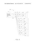
Assignees:
HON HAI PRECISION INDUSTRY CO., LTD.
IPC8 Class: AH05K700FI
USPC Class:
361782
Class name: Printed circuit board connection of components to board having passive component
Publication date: 2012-06-14
Patent application number: 20120147579
Abstract:
A printed circuit board includes a high-speed differential signal control
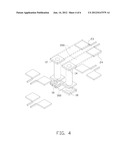
chip, first to eighth coupling capacitor pads, first to fourth connector
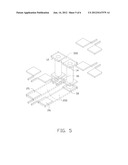
pads, a first transmission line, a second transmission line, a third
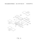
transmission line, a fourth transmission line, first to eighth
transmission lines, two ninth transmission lines, first and second vias,
and first to fourth sharing pads. The printed circuit board is operable
to selectively support multiple connectors.Claims:
1. A printed circuit board (PCB) comprising: a high-speed differential
signal control chip; a first to an eighth coupling capacitor pads; a
first to a fourth connector pads; a first to an eighth transmission lines
and two ninth transmission lines; a first via and a second via; and a
first to a fourth sharing pads; wherein the high-speed differential
signal control chip, the first and second connector pads, the first to
fourth transmission lines, and the first and second sharing pads are
arranged in a first layer, the third and fourth connector pads, the fifth
to eighth transmission lines, and the third and fourth sharing pads are
arranged in a second layer below the first layer, the ninth transmission
lines are arranged in a third layer between the first layer and the
second layer, the first sharing pad is arranged between the first and
third coupling capacitor pads, the second sharing pad is arranged between
the second and fourth coupling capacitor pads, the third sharing pad is
arranged between the fifth and seventh coupling capacitor pads, the
fourth sharing pad is arranged between the sixth and eighth coupling
capacitor pads; wherein the first sharing pad is electrically connected
to the third sharing pad through the first via, the second sharing pad is
electrically connected to the fourth sharing pad through the second via,
the high-speed differential signal control chip is connected to the first
and second vias through the ninth transmission lines; wherein first
terminals of the first and second transmission lines are respectively
connected to two input terminals of the first connector pad, second
terminals of the first and second transmission lines are respectively
connected to the first and second coupling capacitor pads, first
terminals of the third and fourth transmission lines are respectively
connected to two input terminals of the second connector pad, second
terminals of the third and fourth transmission lines are respectively
connected to the third and fourth coupling capacitor pads, first
terminals of the fifth and sixth transmission lines are respectively
connected to two input terminals of the third connector pad, second
terminals of the fifth and sixth transmission lines are respectively
connected to the fifth and sixth coupling capacitor pads, first terminals
of the seventh and eighth transmission lines are respectively connected
to two input terminals of the fourth connector pad, second terminals of
the seventh and eighth transmission lines are respectively connected to
the seventh and eighth coupling capacitor pads; and wherein two first
coupling capacitors are operable to be selectively respectively connected
to the first and second sharing pads and the first and second coupling
capacitor pads, and respectively connected to the first and second
sharing pads and the third and fourth coupling capacitor pads, two second
coupling capacitors are operable to be selectively respectively connected
to the third and fourth sharing pads and the fifth and sixth coupling
capacitor pads, and respectively connected to the third and fourth
sharing pads and the seventh and eighth coupling capacitor pads.
2. The PCB of claim 1, further comprising a bridge capacitor, wherein the bridge capacitor is operable to be connected to the third sharing pads and fourth sharing pads in response to the first and second sharing pads being connected to the first coupling capacitors.
3. The PCB of claim 1, further comprising a bridge capacitor, wherein the bridge capacitor is operable to be connected to the first sharing pads and second sharing pads in response to the third and fourth sharing pads being connected to the second coupling capacitors.
Description:
BACKGROUND
[0001] 1. Technical Field
[0002] The present disclosure relates to printed circuit boards (PCBs) and, particularly, to a PCB selectively supporting four different connectors.
[0003] 2. Description of Related Art
[0004] A computer motherboard includes hard disk drive (HDD) connectors to install HDDs, such as SAS (serial attached SCSI) HDDs and SATA (serial ATA) HDDs. The SAS and SATA HDDs can use a common peripheral component interconnection (PCI) chip for transmitting data, while the motherboard normally only supports connectors of one type, such that layout of the motherboard must be changed when the HDD type is changed, which increases costs.
BRIEF DESCRIPTION OF THE DRAWINGS
[0005] Many aspects of the present embodiments can be better understood with reference to the following drawings. The components in the drawings are not necessarily drawn to scale, the emphasis instead being placed upon clearly illustrating the principles of the present embodiments. Moreover, in the drawings, all the views are schematic, and like reference numerals designate corresponding parts throughout the several views.
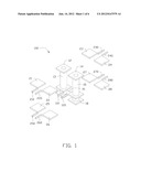
[0006] FIG. 1 is a schematic, isometric view of an embodiment of a printed circuit board (PCB).
[0007] FIG. 2 is a circuit diagram of the PCB of FIG. 1.
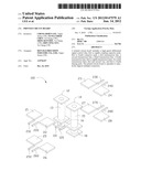
[0008] FIG. 3 is a schematic, isometric view of the PCB of FIG. 1, connected to a first connector pad.
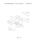
[0009] FIG. 4 is a schematic, isometric view of the PCB of FIG. 1, connected to a second connector pad.
[0010] FIG. 5 is a schematic, isometric view of the PCB of FIG. 1, connected to a third connector pad.
[0011] FIG. 6 is a schematic, isometric view of the PCB of FIG. 1, connected to a fourth connector pad.
DETAILED DESCRIPTION
[0012] The disclosure, including the accompanying drawings, is illustrated by way of example and not by way of limitation. It should be noted that references to "an" or "one" embodiment in this disclosure are not necessarily to the same embodiment, and such references mean at least one.
[0013] Referring to FIGS. 1 and 2, an embodiment of a printed circuit board (PCB) 100 includes a high-speed differential signal control chip 10, first to eighth coupling capacitor pads 21-28, first to fourth connector pads 31-34, ten transmission lines 110, 120, 210, 220, 230, 240, 250, 260, 270, and 280, and first to fourth sharing pads 12, 14, 16, and 18. In one embodiment, the first and second connector pads 31 and 32, the transmission lines 210, 220, 230, and 240, the first to fourth coupling capacitor pads 21-24, and the first and second sharing pads 12 and 14 are arranged in a first layer of the PCB 100. The third and fourth connector pads 33 and 34, the transmission lines 250, 260, 270, and 280, the fifth to eighth coupling capacitor pads 25-28, and the third and fourth sharing pads 16 and 18 are arranged in a second layer of the PCB 100 below the first layer. The transmission lines 110 and 120 are arranged in a third layer between the first layer and the second layer of the PCB 100. The first sharing pad 12 is electrically connected to the third sharing pad 16 through a first via 13. The second sharing pad 14 is electrically connected to the fourth sharing pad 18 through a second via 15. The first to fourth connector pads 31-34 are supported for different types of connectors (not shown), respectively for a first connector, a second connector, a third connector, and a fourth connector.
[0014] The chip 10 is arranged in the first layer or the second layer of the PCB 100. First terminals of the transmission lines 110 and 120 are connected to the chip 10, and second terminals of the transmission lines 110 and 120 are respectively connected to the first via 13 and the second via 15. First terminals of the transmission lines 210 and 220 are connected to two input terminals of the first connector pad 31. Second terminals of the transmission lines 210 and 220 are respectively connected to the first and second coupling capacitor pads 21 and 22. First terminals of the transmission lines 230 and 240 are connected to two input terminals of the second connector pad 32. Second terminals of the transmission lines 230 and 240 are respectively connected to the third and fourth coupling capacitor pads 23 and 24. First terminals of the transmission lines 250 and 260 are connected to two input terminals of the third connector pad 33. Second terminals of the transmission lines 250 and 260 are respectively connected to the fifth and sixth coupling capacitor pads 25 and 26. First terminals of the transmission lines 270 and 280 are connected to two input terminals of the fourth connector pad 34. Second terminals of the transmission lines 270 and 280 are respectively connected to the seventh and eighth coupling capacitor pads 27 and 28.
[0015] The first sharing pad 12 is arranged between the first and third coupling capacitor pads 21 and 23. The second sharing pad 14 is arranged between the second and fourth coupling capacitor pads 22 and 24. The third sharing pad 16 is arranged between the fifth and seventh coupling capacitor pads 25 and 27. The fourth sharing pad 18 is arranged between the sixth and eighth coupling capacitor pads 26 and 28.
[0016] Referring to FIG. 3, when the first connector is installed in the first connector pad 31, the third to eighth coupling capacitor pads 23-28 are void. Two coupling capacitors 200, such as alternating current (AC) coupling capacitors, are respectively connected to the first coupling capacitor pad 21 and the first sharing pad 12, and connected to the second coupling capacitor pad 22 and the second sharing pad 14. A bridge capacitor 300 is connected to the third sharing pad 16 and the fourth sharing pad 18. Thus, high-speed differential signals output by the chip 10 are transmitted to the first connector through the transmission lines 110 and 120, the first and second vias 13 and 15, the first and second sharing pads 12 and 14, the coupling capacitors 200, the first and second coupling capacitor pads 21 and 22, and the transmission lines 210 and 220 in order. The bridge capacitor 300 can decrease signal intensity of the high-speed differential signals output by the chip 10, to increase reliability thereof. In other embodiments, the bridge capacitor 300 can be omitted for conserving costs.
[0017] Referring to FIG. 4, when the second connector is installed in the second connector pad 32, the first, second, and fifth to eighth coupling capacitor pads 21, 22, and 25-28 are void. Two coupling capacitors 200 are respectively connected to the third coupling capacitor pad 23 and the first sharing pad 12, and connected to the fourth coupling capacitor pad 24 and the second sharing pad 14. A bridge capacitor 300 is connected to the third sharing pad 16 and the fourth sharing pad 18. Thus, high-speed differential signals output by the chip 10 are transmitted to the second connector through the transmission lines 110 and 120, the first and second vias 13 and 15, the first and second sharing pads 12 and 14, the coupling capacitors 200, the third and fourth coupling capacitor pads 23 and 24, and the transmission lines 230 and 240 in order.
[0018] Referring to FIG. 5, when the third connector is installed in the third connector pad 33, the first to fourth, seventh, and eighth coupling capacitor pads 21-24, 27, and 28 are void. Two coupling capacitors 200 are respectively connected to the fifth coupling capacitor pad 25 and the third sharing pad 16, and connected to the sixth coupling capacitor pad 26 and the fourth sharing pad 18. A bridge capacitor 300 is connected to the first sharing pad 12 and the second sharing pad 14. Thus, high-speed differential signals output by the chip 10 are transmitted to the third connector through the transmission lines 110 and 120, the first and second vias 13 and 15, the third and fourth sharing pads 16 and 18, the coupling capacitors 200, the fifth and sixth coupling capacitor pads 25 and 26, and the transmission lines 250 and 260 in order.
[0019] Referring to FIG. 6, when the fourth connector is installed in the fourth connector pad 34, the first to sixth coupling capacitor pads 21-26 are void. Two coupling capacitors 200 are respectively connected to the seventh coupling capacitor pad 27 and the third sharing pad 16, and connected to the eighth coupling capacitor pad 28 and the fourth sharing pad 18. A bridge capacitor 300 is connected to the first sharing pad 12 and the second sharing pad 14. Thus, high-speed differential signals output by the chip 10 are transmitted to the fourth connector through the transmission lines 110 and 120, the first and second vias 13 and 15, the third and fourth sharing pads 16 and 18, the coupling capacitors 200, the seventh and eighth coupling capacitor pads 27 and 28, and the transmission lines 270 and 280 in order.
[0020] Thus, the PCB 100 is capable of flexibly supporting different types of connectors according to requirements, to decrease cost.
[0021] It is to be understood, however, that even though numerous characteristics and advantages of the embodiments have been set forth in the foregoing description, together with details of the structure and function of the embodiments, the disclosure is illustrative only, and changes may be made in details, especially in matters of shape, size, and arrangement of parts within the principles of the embodiments to the full extent indicated by the broad general meaning of the terms in which the appended claims are expressed.
User Contributions:
Comment about this patent or add new information about this topic:
| People who visited this patent also read: | |
| Patent application number | Title |
|---|---|
| 20120146237 | SEMICONDUCTOR DEVICE AND METHOD FOR MANUFACTURING THE SAME |
| 20120146236 | Semiconductor Device and Method of Forming Openings Through Insulating Layer Over Encapsulant for Enhanced Adhesion of Interconnect Structure |
| 20120146235 | INTEGRATED CIRCUIT PACKAGING SYSTEM WITH VERTICAL INTERCONNECTION AND METHOD OF MANUFACTURE THEREOF |
| 20120146234 | SEMICONDUCTOR DEVICE PACKAGE AND METHOD OF MANUFACTURING THEREOF |
| 20120146233 | SEMICONDUCTOR DEVICE AND SUBSTRATE |
Images included with this patent application:
 |  |
 |  |
 |  |
 |
| Similar patent applications: | |
| Date | Title |
|---|---|
| 2009-04-16 | Printed circuit board |
| 2009-10-08 | Printed circuit board |
| 2010-02-18 | Printed circuit board |
| 2010-02-25 | Printed circuit board |
| 2010-05-13 | Printed circuit board |
| New patent applications in this class: | |
| Date | Title |
|---|---|
| 2019-05-16 | Systems and methods for an intermediate device structure |
| 2016-06-30 | Composite electronic component |
| 2016-06-16 | Printed electronic components on universally patterned substrate for integrated printed electronics |
| 2016-06-09 | Electronic circuit assembly substrate and device thereof |
| 2016-06-02 | Printed circuit board |
| New patent applications from these inventors: | |
| Date | Title |
|---|---|
| 2015-05-21 | Printed circuit board |
| 2014-10-16 | System and method for checking signal transmission line |
| 2014-09-11 | Control system and method for server |
| 2014-08-21 | Storage expansion system |
| 2014-07-31 | Data center and power supply system thereof |
| Top Inventors for class "Electricity: electrical systems and devices" | |
| Rank | Inventor's name |
|---|---|
| 1 | Zheng-Heng Sun |
| 2 | Levi A. Campbell |
| 3 | Li-Ping Chen |
| 4 | Robert E. Simons |
| 5 | Richard C. Chu |