Patent application title: LOW PROFILE CHIP SCALE MODULE AND METHOD OF PRODUCING THE SAME
Inventors:
Jing-En Luan (Singapore, SG)
Jing-En Luan (Singapore, SG)
Assignees:
STMICROELECTRONICS ASIA PACIFIC PTE LTD
IPC8 Class: AH04N5225FI
USPC Class:
348374
Class name: Camera, system and detail support or housing for internal camera components
Publication date: 2012-05-03
Patent application number: 20120105713
Abstract:
A low profile chip scale module and method of making of the same. The low
profile chip scale module includes embedded SMD and integrated EM
shielding. An adhesive layer is arranged on a substrate, e.g., chip
carrier. Dies and SMDs are arranged on the adhesive layer. An etched
frame and molding is attached to the substrate. Inputs/outputs (I/O) are
formed and the substrate is coated with a dielectric material. Metal
lines and connections among bond pads are formed and another layer of
dielectric material is applied as a protective layer. The substrate is
cut into various predetermined sizes and a lens is attached to form the
chip scale module.Claims:
1. A camera module, comprising: a substrate; an image sensor arranged on
the substrate; a surface mount device (SMD) arranged on the substrate; a
dielectric material substantially covering the SMD and image sensor; a
conductive material in the dielectric material coupling the SMD and the
image sensor; an IR glass assembly coupled to the dielectric material;
and a lens assembly coupled to the IR glass assembly.
2. The camera module of claim 1, wherein the substrate comprises a carrier.
3. The camera module of claim 1, wherein the image sensor comprises a complementary metal oxide semiconductor (CMOS) image sensor.
4. The camera module of claim 1, wherein the image sensor comprises a charged coupled device (CCD) image sensor.
5. The camera module of claim 1, wherein the SMD is selected from the group consisting of capacitors, resistors, inductors and combinations thereof.
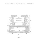
6. The camera module of claim 1, wherein the image sensor has a dimension in a range from about 1.times.1 mm to about 14.times.14 mm.
7. The camera module of claim 1, wherein the camera module has a dimension in a range from about 2.times.2 mm to about 15.times.15 mm.
8. The camera module of claim 1, wherein the lens assembly comprises a lens, a lens holder and lens barrel.
9. The camera module of claim 1, wherein the dielectric material is selected from the group consisting of polyamide, bisbenzocyclobutene (BCB) and combinations thereof.
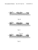
10. A mobile device comprising the camera module of claim 1.
11. A method of making a camera module, comprising the steps of: providing a substrate; providing an adhesive layer on the substrate; arranging a die and surface mount device (SMD) on the adhesive layer; forming a conductive frame on the substrate; molding the frame with a compressive molding material; removing a portion of the frame to form an input/output pattern; forming a first dielectric material on the input/output pattern; releasing the adhesive layer from the substrate; forming a second dielectric material to substantially cover the die and the SMD; forming a conductive material on the dielectric material to electrically couple the SMD and die; and forming a third dielectric material to substantially cover the die, SMD and conductive material.
12. The method of claim 11, further comprising the steps of: dividing the substrate into a plurality of units at predetermined portioned locations; and attaching a lens assembly each of the plurality of units.
13. The method of claim 11, wherein the conductive material comprises a material selected from the group consisting of copper, steel and alloys thereof.
14. The method of claim 11, wherein the molding is normally compression molding with epoxy molding compound.
15. The method of claim 11, wherein the first dielectric material, second dielectric material and third dielectric material comprises a material selected from the group consisting of polyamide and bisbenzocyclobutene (BCB).
16. The method of claim 11, wherein the substrate comprises a carrier substrate.
17. The method of claim 11, wherein the SMD is selected from the group consisting of capacitors, resistors, inductors and combinations thereof.
18. The method of claim 11, wherein the die comprises an image sensor.
19. The method of claim 18, wherein the image sensor is selected from the group consisting of a complementary metal oxide semiconductor (CMOS) image sensor and a charged coupled device (CCD) image sensor.
20. The method of claim 11, wherein the die comprises dimensions in a range from about 1.times.1 mm to about 14.times.14 mm.
21. The method of claim 11, wherein the adhesive layer comprises a thermally releasable adhesive comprises a thermally releasable tape.
Description:
BACKGROUND OF THE INVENTION
[0001] 1. Field of the Invention
[0002] The invention generally relates to chip scale module and methods for making the same, and more particularly to a chip scale module used in a camera module.
[0003] 2. Discussion of the Related Art
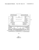
[0004] Camera modules are currently being used in a variety of different mobile terminals, such as portable phones, smart phones, camera phones, personal digital assistants, laptops, and the like. FIG. 1 is a related art camera module. Referring to FIG. 1, the related camera module is generally depicted as reference number 100. The camera module includes a lens module 102, a substrate 104, a die 106, e.g., image sensor, a surface mount device (SMD) 108 and an IR glass 110. The lens module 102 includes a lens holder 112, lens barrel 114, and lens 116. The image sensor may include a complementary metal oxide semiconductor (CMOS) image sensor, charged coupled device (CCD) image sensor or the like. The SMD 108 is directly coupled to the substrate 104 and bonding wires 118. As demand for high quality images increases, the damage for larger dies also increases. At the same time the demand for smaller mobile terminals is also increasing. However, the related art has some limitations due to the space required for wire bonding and places to arrange the SMD as the die increases in size. For example, as the die size increases there is no space for wire bonding or SMDs.
SUMMARY OF THE INVENTION
[0005] Accordingly, the invention is directed to a low profile chip scale module and method of producing the same that substantially obviates one or more of the problems due to limitations and disadvantages of the related art.
[0006] An advantage of the invention is to provide a compact camera module without a bonding wire, thereby, the die size is close to module size.
[0007] Another advantage of the invention is to provide a camera module having a die with dimensions ranging from about 1×1 mm to about 14×14 mm.
[0008] Still yet another advantage of the invention is to provide a camera module having dimensions ranging from about 2×2 mm to about 15×15 mm.
[0009] Yet another advantage of the invention is to provide a camera module having a conductive material coupling the SMD and die integrated into a dielectric material, thereby, significantly reducing the overall dimension of the camera module and also permitting the use of large dies, e.g., dies having dimensions ranging from about 1×1 mm to about 14×14 mm.
[0010] Still yet another advantage of the invention is to provide a camera module having SMDs embedded with the die, e.g., on the same layer/plane as the die.
[0011] Yet another advantage of the invention is to provide a camera module with system integration capability, it can have multi-dice, like sensor, processor to integrate within the camera module.
[0012] Yet another advantage of the invention is to provide a camera module with integrated electromagnetic (EM) shielding.
[0013] Additional features and advantages of the invention are set forth in the description which follows, and in part will be apparent from the description, or may be learned by practice of the invention. The objectives and other advantages of the invention will be realized and attained by the structure particularly pointed out in the written description and claims hereof as well as the appended drawings.
[0014] To achieve these and other advantages and in accordance with the purpose of the invention, as embodied and broadly described, the invention includes a camera module including a substrate and an image sensor and surface mount device (SMD) arranged on the substrate. A dielectric material substantially covers the SMD and image sensor. There is an opening on the dielectric to expose a sensor area of the image sensor. A conductive material in the dielectric material couples the SMD and the image sensor. An IR glass assembly is coupled to the dielectric material and a lens assembly is coupled to the IR glass assembly.
[0015] In another aspect of the invention, the invention is directed towards a method of making a camera module including the steps of providing a substrate and an adhesive layer on the substrate. At least one die and surface mount device (SMD) are arranged on the adhesive layer. A conductive frame also is arranged on the substrate. A molding is applied to the frame with a compressive molding material. A portion of the frame is removed to form an input/output pattern. A first dielectric material is formed on the input/output pattern and the adhesive layer is released from the substrate. Processing is now performed opposite the structure and includes forming a second dielectric material to substantially cover the die and the SMD. A conductive material is formed on the dielectric material electrically coupling the SMD, die and portion of the frame. A third dielectric material is formed to substantially cover the die, SMD and conductive material. In another embodiment of the invention, the camera module is utilized in a mobile device.
[0016] It is to be understood that both the foregoing general description and the following detailed description are exemplary and explanatory and are intended to provide further explanation of the invention as claimed.
BRIEF DESCRIPTION OF THE DRAWINGS
[0017] The accompanying drawings, which are included to provide a further understanding of the invention and are incorporated in and constitute a part of this specification, illustrate embodiments of the invention and together with the description serve to explain the principles of the invention.
[0018] In the drawings:
[0019] FIG. 1 is schematic, cross-sectional view of a camera module, according to the related art;
[0020] FIG. 2 is a schematic, cross-sectional view of a camera module according to an embodiment of the invention; and
[0021] FIGS. 3A-3L are schematic, cross-sectional views illustrating a process flow for forming a camera module according to another embodiment of the invention.
DETAILED DESCRIPTION OF THE ILLUSTRATED EMBODIMENTS
[0022] The invention generally relates to low profile chip scale module and methods for making the same, and more particularly to a packaging method and to a low profile chip scale module. The chip scale module may be used in a camera module and has significant advantages. The chip scale module includes embedded SMDs and EM shielding and is small, e.g., about 2×2 mm to about 15×15 mm. The camera module is configurable to hold dies in a range of about 1×1 mm to about 14×14 mm. The camera module may have a dimension of about 2×2 mm to about 15×15 mm.
[0023] In an embodiment of the invention, the camera module includes a die and surface mount device (SMD) arranged on the substrate. A conductive frame or material is arranged under the die and SMD. The conductive frame includes a conductive material such as copper, steel, alloys and the like. The die may be any type of desired die as known in the art. In a preferred embodiment, the die includes an image sensor, e.g., a complementary metal oxide semiconductor (CMOS) image sensor, charged coupled device (CCD) image sensor or the like. The SMD may include capacitors, resistors, conductors and the like.
[0024] A dielectric material covers the SMD, die and portion of the conductive material. The dielectric material may include epoxy novolacs with rubber filler, such as WPR-5100 series from JSR micro materials innovation, polyamide, bisbenzocyclobutene (BCB) and the like. An opening is formed in the dielectric material to expose an operational area of the die, e.g., sensor area of the image sensor. A conductive material is embedded in the dielectric material and is configured to couple the SMD, die, and conductive material. A protective dielectric material protects the conductive material.
[0025] An IR glass assembly is coupled to the protective dielectric material, and a lens assembly is coupled to the IR glass assembly with adhesive materials. The adhesive materials may include, e.g., epoxy such as Ablebond 8378B, epoxy by Henkel, Ablebond 2030, Loctite 3200 and the like. The lens assembly and lens assembly may be an integral unit. The IR glass assembly includes a lens holder, lens barrel, and lens. The lens may be a plastic lens, a glass lens and the like. The lens is adjustable up and down via the lens barrel.
[0026] The IR glass assembly includes an IR glass shelf configured to hold an IR glass. The IR glass is attached to the lens nook with an adhesive material. The lens assembly is attached to the chip sensor unit with an adhesive material. The lens assembly is attached to the IR glass assembly with an adhesive material.
[0027] Another embodiment of the invention is directed towards a method of making a chip scale unit. The method includes providing a substrate, e.g., carrier, and attaching an adhesive layer to the substrate. The adhesive layer may be a thermal adhesive configured to release at a certain temperature, e.g., thermal release tape such as REVALPHA, thermal release tape from Nitto Denko. A plurality of dies and surface mount devices are also arranged on the adhesive layer. A conductive frame is arranged over the dies and surface mount devices. The conductive frame may include copper, steel, alloys and the like. A molding material is applied to the frame, surface mount devices and dies to encapsulate the same. The molding material may include an epoxy molding, e.g., RH4212 epoxy molding compound from Nogase Corp. of Japan.
[0028] The conductive frame is patterned with techniques known in the art to form a predetermined input/output pattern. The adhesive layer is released by heating to a temperature of about 150° C. to about 200° C. The unit is flipped over for further processing on the reverse side. A second dielectric material is formed to substantially cover the dies and surface mount devices. A portion of the dielectric material is removed to expose a predetermined portion of the dies, e.g., by etching. A conductive material is formed on the dielectric material to electrically couple the dies, surface mount devices and frame. A third dielectric material is formed to substantially cover the die, SMD and conductive material.
[0029] This third dielectric material is a protective layer. The chip scale sensor module is now complete. The first, second and third dielectric materials may be the same or different, e.g., they may include epoxy novolacs with rubber filler, such as WPR-5100 series from JSR micro materials innovation, polyamide, bisbenzocyclobutene (BCB) and the like.
[0030] A lens assembly and IR glass assembly are now attached to the chip scale sensor module to form a camera module. The lens assembly and IR glass assembly may be an integral unit. However, in this embodiment, the lens assembly includes a lens holder, a lens barrel and a lens. The lens barrel is configured to hold a lens and to adjust the focal length of the lens.
[0031] The IR glass assembly includes an IR glass shelf configured to hold an IR glass. The IR glass is attached to the lens shelf with an adhesive material. The lens assembly is attached to the chip sensor unit with an adhesive material, e.g., thermal release tape such as REVALPHA, thermal release tape from Nitto Denko. The lens assembly is attached to the IR glass assembly with an adhesive material. The lens assembly and the IR glass assembly may also be an integral unit, that is, there may be no need for the adhesive material as the structure is one integral piece.
[0032] Reference will now be made in detail to an embodiment of the present invention, an example of which is illustrated in the accompanying drawings.
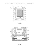
[0033] FIG. 2 is a schematic, cross-sectional view of a camera module according to an embodiment of the invention.
[0034] Referring to FIG. 2, a camera module is generally depicted as reference number 200. The camera module includes a lens assembly 202, IR glass assembly 204 and chip scale sensor unit 206. The lens assembly 202 includes lens holder 210, a lens barrel 208 and a lens 212. The lens barrel is configured to be adjustable such that the focal length of the lens 212 may change.
[0035] The IR glass assembly 204 includes an IR glass holding portion 214 configured to hold an IR glass 216. The IR glass 216 is attached to the holding portion 214 with an adhesive material 218. The IR glass assembly 204 is attached to the chip sensor unit 206 with an adhesive material 220, e.g., epoxy such as Ablebond 8378B, epoxy by Henkel, Ablebond 2030, Loctite 3200 and the like. The lens assembly 202 is attached to the IR glass assembly 204 with an adhesive material 222. The lens assembly 202 and the IR glass assembly 204 may also be on integral unit.
[0036] The chip sensor unit 206 includes a die 224 and at least one SMD 226. The die 224 and SMD 226 are coupled to an input/output array 228 with a patterned conductive material 230 and interconnect 232 embedded in a dielectric material 234.
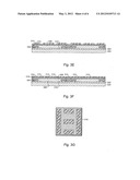
[0037] FIGS. 3A-3K are schematic, cross-sectional views illustrating a process flow for forming a camera module.
[0038] Referring now to FIGS. 3A-3K, a thermally activated adhesive layer 302 is applied to a chip carrier 304. The thermally activated adhesive layer 302 is thermal release tape such as REVALPHA, thermal release tape from Nitto Denko. A SMD 306 is attached to the adhesive layer 302. A die 308 including a bond pad 310 is applied to the adhesive layer 302. As shown, a plurality of SMDs and a plurality of dies may be applied at predetermined locations on the adhesive layer.
[0039] A frame 312 is placed on the adhesive layer to have configuration as shown in FIG. 3C. Molding 314 is then applied as shown in FIG. 3D. It is normally compression molding with liquid molding compound. The frame 312 is further etched with techniques as known in the art to form an input/output pattern 316 as shown in FIGS. 3E and 3G. A dielectric material 315 is then formed in the etched portions of the frame to form an input/output pattern 316 as shown in FIG. 3G. The adhesive layer 302 is now released the overall structure flipped over for processing on the other surface.
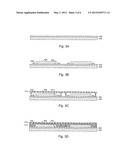
[0040] Referring now to FIG. 3H, a diectric layer 318 is formed on the reverse surface of the structure, i.e., formed on the SMD 306 and die 308. An opening is formed in the dielectric layer to expose a portion of the die 308 and to form vias for connecting to through the dielectric material to the frame 312, SMD 306 and bond pads 310 with techniques as known in the art. A conductive material 320 is then formed on the dielectric layer 318 to electrically couple the frame 312, SMD 306 and bond pad 310 as shown in FIG. 3H and with techniques as known in the art.
[0041] In FIG. 3I, a dielectric layer 322 is formed on the conductive layer 308 to protect the conductive layer. The conductive layer 320 is formed with techniques as know in the art. In FIG. 3J, the overall structure is divided into a plurality of units at predetermined portioned locations thereby forming an individual chip scale sensor unit 324 as shown in FIG. 3K. The chip scale sensor unit 324 includes a sensor area 326 of the die 308. The dividing may be conducted by techniques known in the art, e.g., cutting. Referring now to FIG. 3L, a lens assembly 328 and IR glass assembly 330 are attached to the chip scale sensor unit 324. The lens assembly 328 includes lens holder 334 and a lens barrel 332 configured to be adjustably coupled to the lens holder 334. The lens barrel 332 is configured to hold a lens 336.
[0042] The IR glass assembly 330 includes an IR glass shelf 338 configured to hold an IR glass 340. The IR glass 340 is attached to the lens shelf 338 with an adhesive material 342. The lens assembly 330 is attached to the chip sensor unit 326 with an adhesive material 344, e.g., epoxy. The lens assembly 328 is attached to the IR glass assembly 330 with an adhesive material 346. The lens assembly 328 and the IR glass assembly may also be an integral unit, that is, there may be no need for the adhesive material 346 as the structure is one integral piece.
[0043] It will be apparent to those skilled in the art that various modifications and variations can be made in the present invention without departing from the spirit or scope of the invention. Thus, it is intended that the present invention cover the modifications and variations of this invention provided they come within the scope of the appended claims and their equivalents.
User Contributions:
Comment about this patent or add new information about this topic:
| People who visited this patent also read: | |
| Patent application number | Title |
|---|---|
| 20120121725 | COSMETIC COMPOSITION FOR THE TREATMENT OF ACNE COMPRISING A PEPTIDE EXTRACT OF SCHIZANDRA |
| 20120121724 | FILM COMPRISING THERAPEUTIC AGENTS |
| 20120121723 | Antimicrobial Compositions |
| 20120121722 | ATAZANAVIR FORMULATIONS |
| 20120121721 | SKIN CARE PRODUCTS AND COMPOSITIONS |
Images included with this patent application:
 |  |
 |  |
 |  |
 |
| Similar patent applications: | |
| Date | Title |
|---|---|
| 2011-04-07 | Image sensors and methods of fabricating the same |
| 2011-02-03 | Wafer-level camera module and method for coating the same |
| 2011-03-31 | Television receiver and method of receiving television broadcasting |
| 2011-04-07 | Image sensor module and imaging device including the image sensor module |
| 2011-02-03 | Single gate pixel and operation method of single gate pixel |
| New patent applications from these inventors: | |
| Date | Title |
|---|---|
| 2022-09-08 | Wafer level packaging having redistribution layer formed utilizing laser direct structuring |
| 2021-12-23 | Embedded wafer level optical sensor packaging |
| 2021-12-23 | Wafer level chip scale packaging with sensor |
| 2013-07-04 | Adhesive dam |
| 2012-07-12 | Chip scale package structure with can attachment |
| Top Inventors for class "Television" | |
| Rank | Inventor's name |
|---|---|
| 1 | Canon Kabushiki Kaisha |
| 2 | Kia Silverbrook |
| 3 | Peter Corcoran |
| 4 | Petronel Bigioi |
| 5 | Eran Steinberg |