Patent application title: Method for Manufacturing Vertical Germanium Detectors
Inventors:
Daniel N. Carothers (Oro Valley, AZ, US)
Craig M. Hill (Warrenton, VA, US)
Andrew T.s. Pomerene (Leesburg, VA, US)
Vu A. Vu (Falls Church, VA, US)
Vu A. Vu (Falls Church, VA, US)
Joe Giunta (Warrenton, VA, US)
Jonathan N. Ishii (Fredericksburg, VA, US)
IPC8 Class: AH01L310232FI
USPC Class:
438 69
Class name: Making device or circuit responsive to nonelectrical signal responsive to electromagnetic radiation including integrally formed optical element (e.g., reflective layer, luminescent layer, etc.)
Publication date: 2010-02-04
Patent application number: 20100029033
Inventors list |
Agents list |
Assignees list |
List by place |
Classification tree browser |
Top 100 Inventors |
Top 100 Agents |
Top 100 Assignees |
Usenet FAQ Index |
Documents |
Other FAQs |
Patent application title: Method for Manufacturing Vertical Germanium Detectors
Inventors:
Daniel N. Carothers
Craig M. Hill
Andrew T.S. Pomerene
Vu A. Vu
Joe Giunta
Jonathan N. Ishii
Agents:
BAE SYSTEMS
Assignees:
Origin: NASHUA, NH US
IPC8 Class: AH01L310232FI
USPC Class:
438 69
Patent application number: 20100029033
Abstract:
An improved method for manufacturing a vertical germanium detector is
disclosed. Initially, a detector window is opened through an oxide layer
on a single crystalline substrate. Next, a single crystal germanium layer
is grown within the detector window, and an amorphous germanium layer is
grown on the oxide layer. The amorphous germanium layer is then polished
and removed until only a portion of the amorphous germanium layer is
located around the single crystal germanium layer. A tetraethyl
orthosilicate (TEOS) layer is deposited on the amorphous germanium layer
and the single crystal germanium layer. An implant is subsequently
performed on the single crystal germanium layer. After an oxide window
has been opened on the TEOS layer, a titanium layer is deposited on the
single crystal germanium layer to form a vertical germanium detector.Claims:
1. A method for fabricating a vertical germanium detector, said method
comprising:opening a detector window through an oxide layer on a single
crystalline substrate;growing a single crystal germanium layer within
said detector window, and an amorphous germanium layer on said oxide
layer;polishing and removing said amorphous germanium layer until a
portion of said amorphous germanium layer is located around said single
crystal germanium layer;depositing a dielectric layer on said amorphous
germanium layer and said single crystal germanium layer;performing an
implant on said single crystal germanium layer;opening an oxide window on
said dielectric layer; anddepositing a refractory metal layer on said
single crystal germanium layer to form a germanide layer and a germanium
detector.
2. The method of claim 1, wherein said germanium detector is in a P-i-N configuration.
3. The method of claim 1, wherein said germanium detector includes an underlying n+ silicon layer and a p+ doped germanium layer.
4. The method of claim 1, wherein said germanium detector includes an underlying p+ silicon layer and an n+ doped germanium layer.
5. The method of claim 1, wherein said dielectric layer is a tetraethyl orthosilicate layer.
6. The method of claim 1, wherein said dielectric layer is a germanium oxy-nitride layer.
7. The method of claim 1, wherein said implant is confined within said detector window.
8. The method of claim 1, wherein said refractory metal deposition is confined within said detector window.
9. The method of claim 1, wherein said amorphous germanium layer is completely removed around said single crystal germanium layer.
10. The method of claim 1, wherein said refractory metal deposition is an element selected from the group consisting of titanium, nickel, palladium, platinum, erbium, zirconium, ytterbium, cobalt, zirconium and cobalt.
Description:
PRIORITY CLAIM
[0001]The present application claims benefit of priority under 35 U.S.C. § 365 to the previously filed international patent application number PCT/US08/080471 filed on Oct. 20, 2008, assigned to the assignee of the present application, and having a priority date of Oct. 19, 2007, based upon U.S. provisional patent application No. 60/999,717, the contents of both applications are incorporated herein by reference.
RELATED APPLICATION
[0002]The present application is related to co-pending application Ser. No. 12/201,943 filed on Aug. 29, 2008, the contents of which are incorporated herein by reference.
BACKGROUND OF THE INVENTION
[0004]1. Technical Field
[0005]The present invention relates to optical detectors in general, and in particular to a method for manufacturing vertical germanium detectors.
[0006]2. Description of Related Art
[0007]Photodetection in the near-infrared (IR) regime has many applications, such as telecommunications, thermal imaging, etc. InGaAs-based PIN photodetectors are commonly used for telecommunication applications due to their high responsivity and speed. However, the majority of the InGaAs-based detectors are normal incidence detectors, and the integration of such devices on silicon surfaces can be very expensive. Also, integration of high-speed InGaAs detectors requires special optics to focus light into a small active area, which has been found to reduce device performance.
[0008]Germanium-based detectors are known to be a suitable alternative. However, germanium-based detectors exhibit a higher dark current than InGaAs-based detectors, which limit their application in the telecommunications industry. In recent years, attempts have been made to improve the performance of polycrystalline germanium-based detectors for these applications. One exemplary prior art poly-germanium detector is described by Colace et al. in an article entitled Efficient high-speed near-infrared Ge photodetectors integrated on Si substrates (Applied Physics Letters, vol. 76, p. 1231 et seq., 2000).
[0009]The present disclosure provides an improved method for manufacturing vertical germanium-based detectors.
SUMMARY OF THE INVENTION
[0010]In accordance with a preferred embodiment of the present invention, a detector window is initially opened through an oxide layer on a single crystalline substrate. Next, a single crystal germanium layer is grown within the detector window, and an amorphous germanium layer is grown on the oxide layer. The amorphous germanium layer is then polished and removed until only a portion of the amorphous germanium layer is located around the single crystal germanium layer. A tetraethyl orthosilicate (TEOS) layer is deposited on the amorphous germanium layer and the single crystal germanium layer. An implant is subsequently performed on the single crystal germanium layer. After an oxide window has been opened on the TEOS layer, a titanium layer is deposited on the single crystal germanium layer to form a germanium detector.
[0011]All features and advantages of the present invention will become apparent in the following detailed written description.
BRIEF DESCRIPTION OF THE DRAWINGS
[0012]The invention itself, as well as a preferred mode of use, further objects, and advantages thereof, will best be understood by reference to the following detailed description of an illustrative embodiment when read in conjunction with the accompanying drawings, wherein:
[0013]FIGS. 1-7 illustrate successive steps of a method for fabricating a vertical germanium-based detector, in accordance with a preferred embodiment of the present invention.
DETAILED DESCRIPTION OF A PREFERRED EMBODIMENT
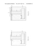
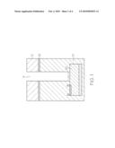
[0014]Referring now to the drawings and in particular to FIGS. 1-7, there are illustrated successive steps of a method for fabricating a vertical germanium-based detector, in accordance with a preferred embodiment of the present invention. Initially, a dry etch process is utilized to open a detector window 11 through a resist layer 12, a nitride layer 13 and an oxide layer 10 on an n+ doped single crystalline substrate having an implant 22 for detectors, as shown in FIG. 1.
[0015]A single crystal germanium layer 14 is then grown within detector window 11, as depicted in FIG. 2. The germanium growth process uses silicon and silicon-germanium seed layers to achieve an abrupt transition to the germanium growth by controlling the surface energy states that the germanium can adhere to as the germanium growth temperature is being modified. The usage of the seed layers allows for a subsequent single crystal germanium growth, even across very large exposed single crystal silicon regions. In addition, the silicon seed layer makes the deposition non-selective to the dielectric region, so an amorphous germanium layer can be grown on top of the oxide mask. This amorphous germanium layer serves as a sacrificial polish layer for subsequent processing. Three different gases are used for the growth of the germanium layer, namely, hydrogen, 100% silane (SiH4), and 100% germane (GeH4). The growth process includes six steps, as follows: [0016]Step 1: Preconditioning with hydrogen at 750° C. for 60 minutes. The pressure is controlled at 3 E-4 mBar. [0017]Step 2: Ramp down to 550° C. in 100 minutes in vacuum at 20° C./min. Silane gas is flowed and controlled at 5 E-4 mBar for 10 minutes. [0018]Step 3: Ramp down to 500° C. in 30 minutes in vacuum at 20° C./min. A 6:4 mixture of silane and germane gases is controlled at 5 E-4 mBar for 30 minutes. [0019]Step 4: A 4:6 mixture of silane and germane gases is controlled at 5 E-4 mBar for 30 minutes. [0020]Step 5: Ramp up to 750° C. in 125 minutes in vacuum at 20° C./min. Hydrogen gas is flowed and controlled at 5 E-4 mBar for 240 minutes. [0021]Step 6: Ramp down to 600° C. in 75 minutes in vacuum at 20° C./min. Germane gas is flowed and controlled at 1.5 E-3 mBar for 600 minutes. 1.5 um of intrinsic single crystal germanium is grown at 600° C.
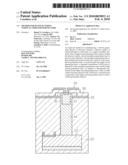
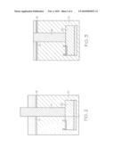
[0022]Single crystal germanium layer 14 and amorphous germanium layer 15 are then polished via a chemical mechanical polish (CMP), as shown in FIG. 3. It is preferable to stop the CMP process before amorphous germanium layer 15 is completely removed. This is because polishing too far can expose voids and crystalline defects that tend to form at the edge of oxide window 11 and single crystal germanium layer 14, and polishing too close to the crystalline defects can create voids by tearing out entire crystalline defects.
[0023]Using a mask, the remaining portion of amorphous germanium layer 15 is removed via a dry etch, leaving a portion of amorphous germanium layer 15 located around single crystal germanium layer 14, as depicted in FIG. 4.
[0024]After a tetraethyl orthosilicate (TEOS) layer 16 has been deposited on amorphous germanium layer 15 and single crystal germanium layer 14, a p+ implant region 17 is created on single crystal germanium layer 14 via a mask and the dopant is activated using an anneal, as shown in FIG. 5. TEOS layer 16 may be replaced by other types of oxides or dielectrics including nitride. For example, germanium oxy-nitride can be used instead of TEOS in layer 16 in order to lower the stress over amorphous germanium layer 15, which should reduce noise and dark current. TEOS layer 16 is utilized to seal the edge of a germanium detector at which defects and voids are most prone to be formed. Preferably, an implant mask is utilized to keep the p+ dopant away from the defects and voids at the edge of single crystal germanium layer 14. Keeping the p+ dopant away from the defect prone edge region decreases detector noise and dark current.
[0025]TEOS (or germanium oxy-nitride) layer 16 is then patterned using a resist mask and a dry etch is utilized to open an oxide window 18, as depicted in FIG. 6. Oxide window 18 exposes germanium regions for a subsequent germanide formation. In order to prevent detector leakage, oxide window 18 must be confined well within p+ doped germanium region 17. Keeping doped germanium region 17 and germanide regions away from the edges of single crystal germanium layer 14 can reduce detector noise and dark current.
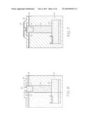
[0026]A titanium deposition is performed on single crystal germanium layer 14 that is exposed through oxide window 18. One or more heat treatments are then used to form a TiGe material 19 within oxide window 18, as shown in FIG. 7. At this point, a P-i-N germanium detector having a vertical configuration is formed, and conventional semiconductor processing techniques may be utilized to fabricate dielectrics and contacts at the top of the P-i-N germanium detector.
[0027]Any un-reacted titanium over TEOS layer 16 can be removed using a resist mask and dry etch. Using a wet process to remove the un-reacted titanium generates concerns of creating voids in the underlying germanium or even removing the germanide itself. The processing options are not limited to titanium germanide as any refractory metal may be used to form the germanide, especially titanium and nickel for underlying p+ germanium, and erbium, zirconium and ytterbium for underlying n+ germanium.
[0028]As has been described, the present invention provides an improved method for manufacturing a vertical germanium detector. Although the process described above is intended for an underlying n+ silicon layer and a p+ doped germanium layer, it is understood by those skilled in the art that the same principle can be applied to an underlying p+ silicon layer and an n+ doped germanium layer.
[0029]While the invention has been particularly shown and described with reference to a preferred embodiment, it will be understood by those skilled in the art that various changes in form and detail may be made therein without departing from the spirit and scope of the invention.
User Contributions:
comments("1"); ?> comment_form("1"); ?>Inventors list |
Agents list |
Assignees list |
List by place |
Classification tree browser |
Top 100 Inventors |
Top 100 Agents |
Top 100 Assignees |
Usenet FAQ Index |
Documents |
Other FAQs |
User Contributions:
Comment about this patent or add new information about this topic:
Images included with this patent application:
 |  |
 |  |
 |
| Similar patent applications: | |
| Date | Title |
|---|---|
| 2009-02-12 | Method for manufacturing vertical mos transistor |
| 2011-02-24 | Method for manufacturing nano-crystalline silicon material for semiconductor integrated circuits |
| 2009-01-01 | Method for manufacturing vertical cmos image sensor |
| 2010-08-12 | Manufacturing method of dynamic random access memory |
| 2011-01-20 | Manufacturing method for planar independent-gate or gate-all-around transistors |
| New patent applications in this class: | |
| Date | Title |
|---|---|
| 2016-05-19 | Method for semiconductor selective etching and bsi image sensor |
| 2016-05-05 | Light-emitting device |
| 2016-04-28 | Semiconductor fabrication method |
| 2016-04-21 | Method of manufacturing semiconductor device, semiconductor device and substrate processing apparatus |
| 2016-04-21 | Grids in backside illumination image sensor chips and methods for forming the same |
| New patent applications from these inventors: | |
| Date | Title |
|---|---|
| 2016-03-10 | Top coupled photonic chip alignment package |
| 2016-01-07 | Method for polishing photonic chips |
| 2015-10-01 | Faceted, germanium slotted waveguide |
| 2015-09-24 | In-line germanium avalanche photodetector |
| Top Inventors for class "Semiconductor device manufacturing: process" | |
| Rank | Inventor's name |
|---|---|
| 1 | Shunpei Yamazaki |
| 2 | Shunpei Yamazaki |
| 3 | Kangguo Cheng |
| 4 | Chen-Hua Yu |
| 5 | Devendra K. Sadana |