Patent application title: Methods Of Forming Structures Supported By Semiconductor Substrates
Inventors:
Anton Devilliers (Boise, ID, US)
Anton Devilliers (Boise, ID, US)
IPC8 Class: AG03F726FI
USPC Class:
430319
Class name: Imaging affecting physical property of radiation sensitive material, or producing nonplanar or printing surface - process, composition, or product making electrical device named electrical device
Publication date: 2009-11-26
Patent application number: 20090291397
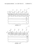
Inventors list |
Agents list |
Assignees list |
List by place |
Classification tree browser |
Top 100 Inventors |
Top 100 Agents |
Top 100 Assignees |
Usenet FAQ Index |
Documents |
Other FAQs |
Patent application title: Methods Of Forming Structures Supported By Semiconductor Substrates
Inventors:
Anton deVilliers
Agents:
WELLS ST. JOHN P.S.
Assignees:
Origin: SPOKANE, WA US
IPC8 Class: AG03F726FI
USPC Class:
430319
Patent application number: 20090291397
Abstract:
Some embodiments include methods of forming structures supported by
semiconductor substrates. Radiation-imageable material may be formed over
a substrate and patterned into at least two separated features. A second
material may be formed over the features and across one or more gaps
between the features. At least one substance may be released from the
features and utilized to alter a portion of the second material. The
altered portion of the second material may be selectively removed
relative to another portion of the second material which is not altered.
Also, the features of radiation-imageable material may be selectively
removed relative to the altered portion of the second material. The
second material may contain one or more inorganic components dispersed in
an organic composition. The substance released from the features of
radiation-imageable material may be acid which forms cross-links within
such organic composition, an hydroxyl, or any other suitable substance.Claims:
1. A method of forming structures, comprising:forming a
radiation-imageable material over a semiconductor
substrate;photolithographically patterning the radiation-imageable
material into at least two separated features; the separated features
having one or more gaps between them;forming a second material over the
at least two separated features, and across the one or more gaps between
the at least two separated features;baking the features having the second
material thereover to release at least one substance which alters the
second material; the non-altered second material being selectively
removable relative to the altered second material, and the features being
selectively removable relative to the altered material; the baking
transferring the at least one substance from the features into regions of
the second material proximate the features to alter said regions while
leaving other regions of the second material non-altered;selectively
removing the non-altered regions of the second material relative to the
altered regions of the second material; andselectively removing the
features relative to the altered regions of the second material to leave
at least one structure of the altered regions of the second material.
2. The method of claim 1 wherein the second material comprises one or more inorganic components dispersed in an organic composition that is cross-linkable upon exposure to acid, wherein the at least one substance released from the features includes acid, and wherein the altering of said regions comprises forming cross-links within the organic composition upon exposure to the acid released from the features.
3. The method of claim 2 wherein the one or more inorganic components include silicon.
4. The method of claim 2 wherein the one or more inorganic components include at least metal.
5. The method of claim 1 wherein:the second material comprises a mixture which includes one or more components dispersed in an organic composition that is cross-linkable upon exposure to acid;the at least one substance released from the features includes acid;the altering of said regions comprises forming cross-links within the organic composition upon exposure to the acid released from the features; andsaid one or more components include one or more of titanium, carbon, fluorine, bromine, silicon and germanium.
6. The method of claim 1 wherein the semiconductor substrate comprises a base semiconductor material and one or more materials over said base semiconductor material; and further comprising utilizing said at least one structure of the altered regions of the second material as a mask during an etch into at least one of said one or more materials.
7. A method of forming structures supported by a semiconductor substrate, comprising:forming at least two separated photoresist features over a semiconductor substrate;forming a material over the at least two photoresist features, and across one or more gaps between the at least two photoresist features; the photoresist features being configured to release at least one substance which alters the material; the non-altered material being selectively removable relative to the altered material, and the photoresist features being selectively removable relative to the altered material;releasing the at least one substance from the photoresist features and into regions of the material proximate the photoresist features to alter said regions; said regions thereby becoming a portion of the material which is altered while another portion of the material remains non-altered;selectively removing the non-altered portion of the material relative to the altered portion of the material; andselectively removing the photoresist features relative to the altered portion of the material to leave at least one structure of the altered portion of the material over the semiconductor substrate.
8. The method of claim 7 wherein the material comprises one or more inorganic components dispersed in an organic composition that is cross-linkable upon exposure to acid, wherein the at least one substance released from the photoresist features includes acid, and wherein the altering of said regions comprises forming cross-links within the organic composition upon exposure to the acid released from the photoresist features.
9. The method of claim 8 wherein the one or more inorganic components include silicon.
10. The method of claim 8 wherein the one or more inorganic components include at least metal.
11. The method of claim 7 wherein:the material comprises a mixture which includes one or more components dispersed in an organic composition that is cross-linkable upon exposure to acid;the at least one substance released from the photoresist features includes acid;the altering of said regions comprises forming cross-links within the organic composition upon exposure to the acid released from the photoresist features; andsaid one or more components include one or more of titanium, carbon, fluorine, bromine, silicon and germanium.
12. The method of claim 7 wherein the semiconductor substrate comprises a base semiconductor material and one or more materials over said base semiconductor material;and further comprising utilizing said at least one structure of the altered portion of the material as a mask during an etch into at least one of said one or more materials.
13. The method of claim 7 wherein said at least one structure of the altered portion of the material comprises a tube.
14. The method of claim 7 wherein said at least one structure of the altered portion of the material comprises a plurality of non-tubular pedestals.
15. The method of claim 7 wherein the altered portion of the material extends over the photoresist features; and further comprising, prior to the selective removal of the photoresist feature relative to the altered portion of the material, removing the altered portion of the material from over the photoresist features while leaving the altered portion of the material along sidewalls of the photoresist features.
Description:
TECHNICAL FIELD
[0001]Methods of forming structures supported by semiconductor substrates.
BACKGROUND
[0002]Integrated circuit fabrication may involve formation of a photolithographically-patterned mask over a semiconductor substrate, followed by transfer of a pattern from the mask into one or more materials with one or more etches.
[0003]The photolithographically-patterned mask may comprise any suitable radiation-imageable material, such as polyimide or photoresist. A pattern is formed in the radiation-imageable material by subjecting the material to patterned actinic radiation (for instance, ultraviolet light) so that some portions of the radiation-imageable material are exposed to the radiation while other portions are not exposed. Either the exposed or unexposed portions may be selectively removed relative to the other of the exposed and unexposed portions with an appropriate developing solution, thereby creating a pattern in the radiation-imageable material.
[0004]A continuing goal of integrated circuit fabrication is to create smaller structures. Numerous difficulties may be encountered in attempting to create smaller structures with traditional photolithographic processing, in that a minimum size achievable by a photolithographic process is imposed by the wavelength of actinic radiation utilized in the process. Modern processes are approaching the limits of scalability imposed by the physical properties of the actinic radiation.
[0005]It would be desired to develop new methods of forming patterns for integrated circuit fabrication which can extend the limits of scalability.
BRIEF DESCRIPTION OF THE DRAWINGS
[0006]FIGS. 1-7 are diagrammatic, cross-sectional views of a portion of a semiconductor wafer construction shown at various process stages of an embodiment.
[0007]FIGS. 8-10 are three-dimensional views of a portion of a semiconductor wafer construction shown at various process stages of an embodiment.
[0008]FIGS. 11 and 12 are views of the portion of FIGS. 1-7 shown at various process stages of an embodiment. The processing stage of FIG. 11 follows that of FIG. 1, and the processing stage of FIG. 12 follows that of FIG. 11.
DETAILED DESCRIPTION OF THE ILLUSTRATED EMBODIMENTS
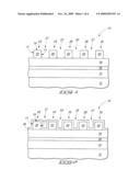
[0009]Example embodiments are described with reference to FIGS. 1-10.
[0010]Referring to FIG. 1, such illustrates a portion of a semiconductor construction 10. The construction includes a base, or substrate, 12, which may, for example, comprise, consist essentially of, or consist of monocrystalline silicon lightly-doped with background p-type dopant. The terms "semiconductive substrate" and "semiconductor substrate" mean any construction comprising semiconductive material, including, but not limited to, bulk semiconductive materials such as a semiconductive wafer (either alone or in assemblies comprising other materials thereon), and semiconductive material layers (either alone or in assemblies comprising other layers). The term "substrate" refers to any supporting structure, including, but not limited to, the semiconductive substrates described above.
[0011]A plurality of materials 14, 16 and 18 are over base 12. The materials may comprise any compositions which may be utilized in forming integrated circuitry. Accordingly, one or more of the materials may comprise an electrically insulative composition (for instance, silicon dioxide, silicon nitride, borophosphosilicate glass, etc.); one or more of the materials may comprise an electrically conductive composition (for instance, metal, metal nitride, metal silicide, conductively-doped silicon, etc.); and/or one or more of the materials may comprise a semiconductor composition (for instance, silicon, germanium, etc.). The materials 14, 16 and 18 may comprise any suitable thicknesses.
[0012]A photolithographically patterned radiation-imageable material 20 is over material 18. Material 20 may, for example, comprise, consist essentially of, or consist of photoresist. The material 20 is patterned into a plurality of separate features 22, 24, 26, 28 and 30; and such features are spaced from one another by gaps 21, 23, 25 and 27. Although five separate features are shown, any suitable number of features may be utilized. Generally, there will be at least two separate features, and accordingly there will generally be at least one gap.
[0013]In the shown cross-sectional view, each of the features has a pair of opposing sidewalls 17 (only labeled for feature 22) and a top 19 (only labeled for feature 22).
[0014]Referring to FIG. 2, a material 40 is formed over the features 22, 24, 26, 28 and 30; and within (or in other words, across) the gaps 21, 23, 25 and 27 between the features. Material 40 may be referred to as a second material to distinguish it from the radiation-imageable material 20.
[0015]Material 40 may be similar to a class of materials available from Clariant International, Ltd. as so-called "AZ R" materials, such as the materials designated as AZ R200®, AZ R500® and AZ R600®.
[0016]The "AZ R" materials contain organic compositions which cross-link upon exposure to acid released from chemically-amplified resist. Specifically, an "AZ R" material may be coated across photoresist, and subsequently the resist may be baked at a temperature of from about 100° C. to about 120° C. to diffuse acid from the resist and into the material to form chemical cross-links within regions of the material proximate the resist. Portions of the material adjacent the resist are thus selectively hardened relative to other portions of material that are not sufficiently proximate the resist. The material may then be exposed to conditions which selectively remove the non-hardened portions relative to the hardened portions. Such removal may be accomplished utilizing, for example, 10% isopropyl alcohol in the ionized water, or a solution marketed as "SOLUTION C®" by Clariant International, Ltd. The processes utilizing the "AZ R" materials are sometimes considered examples of RELACS (Resolution Enhancement Lithography Assisted by Chemical Shrink) processes.
[0017]A problem with the "AZ R" materials can be that they are similar enough in composition to photoresist that it is difficult to selectively remove photoresist relative to the hardened "AZ R" materials.
[0018]Material 40 may be similar to the "AZ R" materials in that it may comprise a similar or identical organic composition which is altered (for instance, forms cross-links) upon exposure to one or more substances (for instance, acid) released from radiation-imageable material when the material is baked. However, unlike the "AZ R" materials, material 40 may also contain one or more components dispersed in the organic composition which are provided to chemically change material 40 relative to radiation-imageable materials (for instance, photoresist) so that the radiation-imageable materials may be selectively removed relative to material 40. The components dispersed in the organic composition of material 40 may include one or more of titanium, carbon, fluorine, bromine, silicon and germanium. The carbon dispersed in the organic composition may be part of a carbide compound so that it is chemically different from the bulk carbon of the organic composition. The fluorine and bromine may be, for example, comprised by hydrofluoric acid and hydrobromic acid. In some embodiments, the components dispersed in the organic composition of material 40 include one or more inorganic components, such as, for example, silicon, germanium, metals (for instance, titanium, tungsten, platinum, etc.) and/or metal-containing compounds (for instance, metal nitride, metal silicide, etc.).
[0019]The component of material 40 that is similar to "AZ R" materials may be referred to as an "AZ R"-type composition. Accordingly, in some embodiments material 40 may be considered to have one or more inorganic components dispersed in an organic "AZ R"-type composition.
[0020]Material 40 may be formed over and between the features 22, 24, 26, 28 and 30 with any suitable methodology, including, for example, spin coating.
[0021]Referring to FIG. 3, construction 10 is subjected to conditions which cause at least one substance to diffuse from material 20 of features 22, 24, 26, 28 and 30 into regions of material 40 proximate such features. The substance alters material 40 to form altered regions 42 proximate the features 22, 24, 26, 28 and 30, and to leave non-altered regions 44 as segments of material 40 that are less proximate the features. The altered regions are designated by cross-hatching in FIG. 3 to emphasize the different regions 42 and 44. The altered regions may be considered together to define an altered portion of material 40, and the non-altered regions may be considered together to define a non-altered portion of material 40.
[0022]In some embodiments, material 20 comprises chemically-amplified photoresist, and the substance diffused from such photoresist is acid. The acid is caused to be released from the photoresist by baking construction 10 at a temperature of at least about 100° C. The acid forms cross-links within the "AZ R"-type composition of material 40. The amount of cross-linking, and the distance that the cross-linking spreads from a photoresist feature, may be adjusted by modifying one or both of the bake time and the bake temperature.
[0023]The non-altered regions 44 of material 40 are selectively removable relative to the altered regions 42, and FIG. 4 shows construction 10 after the non-altered regions have been removed. Such removal may be accomplished utilizing isopropyl alcohol and/or SOLUTION C®. As discussed above, material 40 may comprise various additional components (for instance, metal, silicon dioxide, etc.) dispersed in an "AZ R"-type composition. In some embodiments, the additional components may simply rinse away as the non-altered regions of material 40 are removed. In other embodiments, such additional components may be removed with solvent specific for the additional components. For instance, if silicon dioxide is utilized as a component of material 40, hydrofluoric acid may be utilized during removal of the non-altered regions of material 40 to ensure that the silicon dioxide of the non-altered regions is removed in addition to the "AZ R"-type composition of the non-altered regions.
[0024]The altered regions 42 of material 40 form caps extending over the tops 19 and sidewalls 17 of features 22, 24, 26, 28 and 30. In some embodiments, the features having the caps associated therewith may be utilized for patterning one or more of underlying materials 14, 16 and 18. In other embodiments, it may be desired to selectively remove radiation-imageable material 20 to leave structures comprising only the altered regions 42 of material 40. A method for selectively removing the radiation-imageable material is described with reference to FIGS. 5 and 6.
[0025]Referring to FIG. 5, material 40 is removed from over the tops 19 of features 22, 24, 26, 28 and 30, while leaving material 40 along the sidewalls 17 of such features. The removal of material 40 from over the tops of the features may be accomplished utilizing any suitable processing, including, for example, a directional physical etch and/or chemical-mechanical polishing (CMP).
[0026]Referring to FIG. 6, radiation-imageable material 20 (FIG. 5) is removed to leave structures 50, 52, 54, 56, 58, 60, 62, 64, 66 and 68 of the altered regions 42 of material 40 over material 18. Such structures are double-pitch relative to an original pitch of the features 22, 24, 26, 28 and 30 (FIG. 1) of radiation-imageable material 20.
[0027]Material 20 (FIG. 5) may be selectively removed relative to altered regions 42 of material 40 due to such altered regions comprising one or more components in addition to an "AZ R"-type composition. For instance, if the additional components are resistant to oxidation, the photoresist may be removed utilizing ashing or another oxidative process. Such process may weaken the regions 42 of material 40 due to removal of some of the "AZ R"-type composition. However, the additional components can form a matrix which remains after removal of at least some of the "AZ R"-type composition from the regions 42 of material 40.
[0028]The structures of regions 42 of material 40 may be utilized as a mask. For instance, the structures may be utilized during doping of material 18 to protect a region of the material while another region is doped; and/or the structures may be utilized during one or more etches into one or more of the underlying materials 14, 16 and 18 to define a pattern which is to be formed in such underlying materials.
[0029]FIG. 7 shows construction 10 after structures 50, 52, 54, 56, 58, 60, 62, 64, 66 and 68 have been utilized as a mask during an etch through underlying materials 14, 16 and 18.
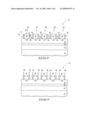
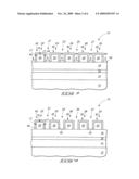
[0030]The processing of FIGS. 2-5 utilizes a thin, conformal coating of material 40 (with material 40 being the material that may be an "AZ R"-type composition). In other embodiments, a thick layer of material 40 may be formed to fill gaps 21, 23, 25 and 27, and to cover features 22, 24, 26, 28 and 30. An example of such other embodiments is shown in FIG. 11, where construction 10 is shown at a processing stage subsequent to that of FIG. 1. The structure of FIG. 11 is at a processing stage analogous to that of FIG. 3, and thus material 40 is sub-divided amongst altered regions 44 and non-altered regions 42. In subsequent processing, the non-altered regions 42 and the upper portions of the altered regions 44 may be removed, to form the construction of FIG. 12. The construction of FIG. 12 is identical to that of FIG. 5. The removal of the non-altered regions 42 and the upper portions of the altered regions 44 may comprise two separate steps, analogous to the steps of FIGS. 4 and 5, or may be conducted in a single step.
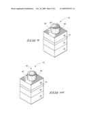
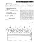
[0031]The structures 50, 52, 54, 56, 58, 60, 62, 64, 66 and 68 of FIGS. 6 and 7 are in the form of pedestals in the shown cross-sectional views. Such pedestals may be part of walls (or lines) extending into and out of the page relative to the shown cross-sectional views. Regardless, the pedestals are non-tubular. In other embodiments, methodology similar to that of FIGS. 1-6 may be utilized to form tubular structures. FIGS. 8-10 illustrate an example of an embodiment that may be utilized for forming tubular structures. Similar numbering will be used to describe FIGS. 8-10 as is used above to describe FIGS. 1-6.
[0032]Referring to FIG. 8, such shows a three-dimensional view of construction 10 at a processing stage analogous to that of FIG. 1. However, unlike FIG. 1, the radiation-imageable material 20 is shown patterned as a cylinder.
[0033]Referring next to FIG. 9, construction 10 is shown at a processing stage subsequent to that of FIG. 8 and analogous to that of FIG. 5. The material 40 has been formed around radiation-imageable material 20 and subjected to processing which forms an altered region 42. Subsequently, the material 40 has been removed from over radiation-imageable material 20 to leave altered region 42 as a tube extending around the cylindrically-shaped radiation-imageable material 20.
[0034]Referring next to FIG. 10, material 20 is removed to leave a structure 70 of an altered region 42 of material 40, with structure 70 being a tube (in other words, a hollow cylinder) over material 18. In subsequent processing (not shown), the tube may be utilized to define a masking pattern for doping and/or etching into underlying materials. The shown tube may be representative of a plurality of tubes simultaneously formed over a semiconductor base.
[0035]The processing of FIGS. 1-10 may be utilized in any of numerous integrated circuitry fabrication applications. For instance, the processing may be utilized to form FLASH memory or dynamic random access memory (DRAM). The processing may be useful for imaging in the less than 35 nanometer (nm) range; such as imaging from about 10 nm to less than 35 nm.
[0036]In compliance with the statute, the subject matter disclosed herein has been described in language more or less specific as to structural and methodical features. It is to be understood, however, that the claims are not limited to the specific features shown and described, since the means herein disclosed comprise example embodiments. The claims are thus to be afforded full scope as literally worded, and to be appropriately interpreted in accordance with the doctrine of equivalents.
User Contributions:
comments("1"); ?> comment_form("1"); ?>Inventors list |
Agents list |
Assignees list |
List by place |
Classification tree browser |
Top 100 Inventors |
Top 100 Agents |
Top 100 Assignees |
Usenet FAQ Index |
Documents |
Other FAQs |
User Contributions:
Comment about this patent or add new information about this topic:
| People who visited this patent also read: | |
| Patent application number | Title |
|---|---|
| 20090310680 | Method and Apparatus for Decoding/Encoding a Video Signal |
| 20090310679 | VIDEO PROCESSING APPARATUS AND METHODS |
| 20090310678 | IMAGE ENCODING APPARATUS, METHOD OF CONTROLLING THE SAME AND COMPUTER PROGRAM |
| 20090310677 | IMAGE ENCODING AND DECODING METHOD AND APPARATUS |
| 20090310676 | PROCESSING MULTIVIEW VIDEO |
Images included with this patent application:
 |  |
 |  |
 |  |
 |
| New patent applications from these inventors: | |
| Date | Title |
|---|---|
| 2015-12-03 | Epitaxial devices |
| 2014-09-25 | Methods for epitaxial devices |
| 2014-09-04 | Lithography wave-front control system and method |
| 2014-04-17 | Lithography methods, methods for forming patterning tools and patterning tools |
| 2014-02-27 | Anti spacer process and semiconductor structure generated by the anti spacer process |
| Top Inventors for class "Radiation imagery chemistry: process, composition, or product thereof" | |
| Rank | Inventor's name |
|---|---|
| 1 | Jun Hatakeyama |
| 2 | Jin Wu |
| 3 | Koji Hasegawa |
| 4 | Yoshiyuki Utsumi |
| 5 | Richard P.n. Veregin |