Patent application title: METHOD OF MAKING A COATED CUTTING TOOL AND CUTTING TOOL THEREOF
Inventors:
Toril Myrtveit (Kungsangen, SE)
Assignees:
Sandvik Intellectual Property AB
IPC8 Class: AB22F702FI
USPC Class:
428545
Class name: Stock material or miscellaneous articles all metal or with adjacent metals component of composite having metal continuous phase interengaged with nonmetal continuous phase
Publication date: 2009-07-02
Patent application number: 20090169910
Inventors list |
Agents list |
Assignees list |
List by place |
Classification tree browser |
Top 100 Inventors |
Top 100 Agents |
Top 100 Assignees |
Usenet FAQ Index |
Documents |
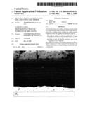
Other FAQs |
Patent application title: METHOD OF MAKING A COATED CUTTING TOOL AND CUTTING TOOL THEREOF
Inventors:
Toril MYRTVEIT
Agents:
DRINKER BIDDLE & REATH (DC)
Assignees:
SANDVIK INTELLECTUAL PROPERTY AB
Origin: WASHINGTON, DC US
IPC8 Class: AB22F702FI
USPC Class:
428545
Abstract:
The invention relates to a method of making a coated cutting tool
comprising providing a substrate, and coating said substrate with a
coating process wherein the coating process comprises at least one
sequence comprising the steps of: depositing a non-metallic, functional
layer or layer system, subjecting the surface of said non-metallic layer
or layer system to an ion etching step, depositing at least one metallic
interlayer, prior to the beginning of a new sequence.
The method according to the invention makes it possible to achieve cutting
tools with an increased tool life time. The invention also relates to a
coated cutting tool made according to the method.Claims:
1. A method of making a coated cutting tool comprising providing a
substrate and coating said substrate with a coating process which
comprises at least one sequence comprising the steps of:depositing a
non-metallic, functional layer or layer system,subjecting the surface of
said non-metallic layer or layer system to an ion etching step,depositing
at least one metallic interlayer.
2. A method of claim 1 wherein the ion etching step is performed with argon ions.
3. A method of claim 1 wherein the ion etching step is performed with metal ions.
4. A method of claim 1 wherein the coating process is either PVD or PECVD.
5. A method of claim 1 wherein the metallic interlayer is a pure metal layer where the metal(s) are chosen from Ti, Mo, Al, Cr, V, Y, Nb, Hf, W, Ta, Zr or any mixture thereof.
6. A method of claim 1 wherein the metallic interlayer is a substoichiometric ceramic wherein the amount of the metal element is at least about 60 at % of the substoichiometric ceramic.
7. A method of claim 6 wherein the substoichiometric ceramic is an nitride, MeN where Me is a metal that is one or more of Ti, Mo, Al, Cr, V, Y, Nb, Hf, W, Ta, Zr, or mixtures thereof.
8. A method of claim 1 wherein the composition of the deposited, non-metallic layers or layer systems, is nitrides, oxides, borides, carbides, or combinations thereof, preferably one or more of (Al,Ti)N, TiN, Ti(C,N), (Al,Cr)N, CrN, Al2O3, Ti(B,N), TiB2, (Zr,Al)N, (Ti,X)N, where X can be one or more of Si, B, C, Ta, V, Y, Cr, Hf, Zr.
9. A method of claim 1 wherein the thickness of the metallic layers is from about 5 to about 500 nm.
10. A method of claim 1 wherein the thickness of the non-metallic layer or layer systems is from about 3 to about 200 times the thickness of the metallic interlayers.
11. A method of claim 1 wherein the total coating thickness is from about 0.5 to about 15 μm.
12. A cutting tool made according to the method of claim 1.
Description:
CROSS-REFERENCE TO PRIOR APPLICATION
[0001]This application claims priority to Sweden Application No. SE 0702866-5 filed Dec. 21, 2007, which is incorporated by reference herein.
BACKGROUND OF THE INVENTION
[0002]The present invention relates to a method of making a coated cutting tool comprising depositing one or more metallic interlayers in-between deposition of two non-metallic, functional layers. Before each deposition of a metal interlayer, an ion etching step of the non-metallic functional layer is performed. The cutting tools made according to the method of the present invention will exhibit superior life time due to an increased toughness, thus showing better ability to withstand changes in load. In addition, this invention facilitates deposition of thicker PVD coatings without the risk of spalling along the edge line, hence thicker coatings with better flank wear resistance can be deposited.
[0003]In general, the life time of a cutting tool is significantly prolonged if a coating is deposited onto its surface. Most cutting tools today are coated with PVD or CVD coatings like Ti(C,N), TiN, (Ti,Al)N, (Ti,Si)N, (Al,Cr)N or Al2O3. PVD coatings have several attractive properties compared to CVD coatings, for instance a residual compressive stress in the as-deposited state, no cooling cracks and finer grained coatings.
[0004]However, the PVD coatings usually have to be quite thin, since thicker PVD coatings may cause spalling, frittering, so-called edge-line spalling and flaking, either spontaneously, usually around the edge line, or during machining. Since thicker coatings in many applications lead to a longer tool life due to an increased wear resistance, CVD coatings are usually chosen for those applications.
[0005]Unfortunately, PVD-coatings, especially arc deposited, suffer from the existence of so-called macros or droplets, which exists as small spheres on the surface of the coating or, buried inside the coating. During the deposition of the coating, these droplets can shadow the incoming flux of charged metal ions, thus creating voids in the coating in the immediate surroundings of the droplet. Due to the subsequent diminished adhesion between the droplet and the coating, the droplet can fall out either during the deposition process or immediately afterwards or even during machining. This may result in an inferior coating quality, with voids, pores or even, in extreme cases, holes straight down to the substrate.
[0006]Thicker coatings also have the advantage that the maximum temperature that the substrate is exposed to decreases. A lower substrate temperature decreases the risk of plastic deformation of the cutting edge. Thicker coatings allow for higher cutting forces without initializing plastic substrate deformation.
[0007]In the business of cutting tools there is a growing demand for thicker PVD coatings experiencing both the advantages in wear resistance of a thicker coating combined with the toughness of a PVD coating.
[0008]Ion etching is a common initial step in the beginning of all kinds of deposition processes. The substrate is usually ion etched prior to deposition to remove surface contaminants and native oxides and nitrides. However, few attempts have been done to use ion etching as an intermediate step.
[0009]Depositing metallic layers with PVD techniques is also an established technology in PVD-processes. It is well-known that depositing a metallic layer directly onto the surface of the substrate before depositing the rest of the coating can in some cases enhance adhesion of the coating.
[0010]EP 0756019 describes a method of making a PVD-coating for material deforming tools used in punching operations. A PVD-layer composed of (Ti,Al)N, (Ti,Al,Y)N or (Ti,Al,Cr)N or any multilayer thereof is deposited. The surface is then mechanically treated e.g. with sand blasting or metal ion etching to remove any droplets and to achieve a smooth surface. A second, low-friction, PVD coating consisting of MoS2 is then deposited on top.
[0011]U.S. Pat. No. 3,755,866 describes an insert comprising two non-metallic interlayers deposited on top of each other. One layer consists of a fine-grained member of the group consisting of TiC, TaC, ZrC, HfC, VC and NbC. The other layer consists of at least one fine grained member of the group consisting of WC, MoC and CrC. These two layers may or may not be separated by a metallic layer consisting of Co, Ni or Fe. The metallic layer is between 0.1 and 2.0 μm.
[0012]EP1136585 describes a self-lubricating coating, consisting of small droplets of metal or other soft material in an otherwise hard coating. Thus, a coating with lower levels of friction is created. The coating is deposited in a sequence consisting of: deposition of a nitride/carbide, followed by ion etching in Ar atmosphere. During the ion etching step a thin metal foil is bombarded with Ar ions, and small metal droplets are emitted. This coating thus consists of layers with small droplets of metal in an otherwise hard coating of a nitride or carbide.
[0013]JP2002-103122A describes hard-anodic-oxidation-coatings covering small diameter tools, where the coating consist of an inner Ti layer, followed by a TiCN-layer, an intermediate metallic TiAl-layer and finally covered by an outer TiAlCN-layer.
[0014]EP1553210 A1 discloses a method of depositing α-Al2O3 layers by PVD technique. In one embodiment, a substrate possibly provided with a primary coating is ion bombarded with either gas ions or metal ions, followed by oxidation of the bombarded surface and finally deposition of a α-Al2O3 layer. When metal ions are used for the bombardment, metal ions are implanted into the surface.
OBJECTS AND SUMMARY OF THE INVENTION
[0015]It is an object of the present invention to provide a method of making a coated cutting tool having a PVD-coating with improved edge toughness.
[0016]It is another object of the present invention to provide a method of making a coated cutting tool having thicker PVD-coatings without increasing the risk of spalling, frittering, so-called edge-line spalling and flaking thus obtaining a tool with an increased tool life.
[0017]It is another object of the present invention to provide a method of making a coated cutting tool having better flank wear resistance.
[0018]It is another object of the present invention to provide a coated cutting tool made according to the method of the invention having the benefits disclosed above.
[0019]In one aspect of the invention, there is provided a method of making a coated cutting tool comprising providing a substrate and coating said substrate with a coating process which comprises at least one sequence comprising the steps of: depositing a non-metallic, functional layer or layer system, subjecting the surface of said non-metallic layer or layer system to an ion etching step, and depositing at least one metallic interlayer.
[0020]In another aspect of the invention, there is provided a cutting tool made by the above-described process.
BRIEF DESCRIPTION OF THE DRAWING
[0021]FIG. 1 shows a SEM-picture of a polished cross section showing thin metallic interlayers inside the coating. The metallic interlayers are placed every 0.7-1.5 μm distance, the total thickness of the coating is 10 μm.
DETAILED DESCRIPTION OF THE PREFERRED EMBODIMENTS
[0022]It has surprisingly been found that, when a non-metallic functional layer is subjected to an ion etching step prior to deposition of a metallic interlayer, the amount of so called droplets inside and on the surface of the non-metallic functional layer is reduced, and in combination with the deposition of the metallic interlayer, the objects above can be fulfilled.
[0023]The present invention relates to a method of making a coated cutting tool comprising providing a substrate and coating said substrate with a coating process comprising at least one sequence comprising the steps of: [0024]depositing a non-metallic, functional layer or layer system, [0025]subjecting the surface of said non-metallic layer or layer system to an ion etching step, [0026]depositing at least one metallic interlayer, prior to the beginning of a new sequence.
[0027]The three steps, as described above are herein after named a sequence, may be repeated any number of times until the desired total coating thickness is achieved.
[0028]The number of sequences is preferably between about 1 and about 20, more preferably between about 1 and about 10, more preferably between about 2 and about 10 and most preferably between about 3 and about 10.
[0029]In one embodiment of the present invention, the final deposition step in the coating process is deposition of a non-metallic layer or layer system.
[0030]In one embodiment of the present invention, a deposition sequence further comprises, after the ion etching step, deposition of a thin non-metallic layer prior to deposition of the metallic interlayer.
[0031]All layers are preferably deposited in the same coating process.
[0032]The ion etching step is achieved by ion bombardment with, for example, argon ions or metal ions.
[0033]In one embodiment of the present invention, argon ions are used. The argon ions are created by igniting plasma in the deposition chamber which is filled with argon. The argon ions are accelerated towards the substrates which are being kept at a negative potential with a value of preferably from about 50 to about 300 V, more preferably from about 100 to about 300 V. The pressure during the etching step is preferably from about 1 to about 15 μbar, more preferably from about 1 to about 5 μbar, the temperature is the same as during deposition, preferably from about 300 to about 800° C., more preferably from about 450 to about 750° C.
[0034]In another embodiment of the present invention, metal ions are used. The deposition chamber is filled with argon, and an arc is ignited at a metal target, thus forming a dense vapor of metal ions. These metal ions are accelerated towards the substrates which are being kept at a high negative potential. The metal ions are preferably one or more of Ti, Zr, Cr, Nb, V, Mo, most preferably Cr. The substrate bias during the metal ion etching step is negative with a value of preferably from about 300 to about 2000 V, more preferably from about 500 to about 1300 V. The pressure during the etching step is preferably from about 1 to about 15 μbar, more preferably from about 1 to about 5 μbar, the temperature is the same as the same as during deposition, preferably from about 300 to about 800° C., more preferably from about 450 to about 750° C.
[0035]After the ion etching step, the metallic interlayer is deposited using the same coating process as for the non-metallic layers by changing the atmosphere to an inert gas, e.g. He, Ar, Kr, Xe or a combination of these gases.
[0036]By metallic interlayer is herein meant a layer comprising at least about 60 at %, preferably 70 at %, more preferably at least about 80 at % and most preferably at least about 90 at % metal elements chosen from one or more of Ti, Mo, Al, Cr, V, Y, Nb, Hf, W, Ta and Zr.
[0037]The deposited metallic interlayers can also comprise smaller amounts of other elements but then at a level corresponding to a technical impurity thus not significantly affecting the ductility of the layers.
[0038]In one embodiment of the present invention, the metallic interlayer is a pure metal layer where the metal(s) are chosen from Ti, Mo, Al, Cr, V, Y, Nb, Hf, W, Ta, Zr, preferably Ti, Mo, Al, V, Ta, Zr, Cr, most preferably Ti, Al, Zr, Cr, or mixtures thereof, where one of these elements constitute at least about 50 at % of the pure metal layer.
[0039]In another embodiment of the present invention, the metallic interlayer is a substoichiometric ceramic, preferably a nitride, oxide, carbide or boride, more preferably a nitride MeN, where Me is a metal that can be one or more of the metals included in the case of a pure metal interlayer as described above. The amount of the metal element is at least about 60 at %, preferably 70 at %, more preferably at least about 80 at % and most preferably at least about 90 at % of the substoichiometric ceramic.
[0040]The average thickness of the metallic interlayers is preferably from about 5 nm to about 500 nm, more preferably from about 10 nm to about 200 nm and most preferably from about 20 nm to about 70 mm.
[0041]All thicknesses given herein refer to measurements conducted on a reasonably flat surface being in direct line of sight from the targets. For inserts, being mounted on sticks during deposition, it means that the thickness has been measured on the middle of the flank side. For irregular surfaces, such as those on e.g. drills and end mills, the thicknesses given herein refers to the thickness measured on any reasonably flat surface or a surface having a relatively large curvature and some distance away from any edge or corner. For instance, on a drill, the measurements have been performed on the periphery and on an end mill the measurements has been performed on the flank side.
[0042]The non-metallic functional layers or layer systems can have any composition suitable for cutting tools, such as nitrides, oxides, borides, carbides, or combinations thereof. Preferably the coating comprises one or more layers of one or more of (Al,Ti)N, TiN, (Al,Cr)N, CrN, Al2O3, Ti(B,N), TiB2, (Zr,Al)N, (Ti,X)N, more preferably (Al,Ti)N, Ti(B,N), (Ti,X)N, where X can be one or more of Si, B, C, Ta, V, Y, Cr, Hf, Zr, and most preferably (Al,Ti)N.
[0043]The non-metallic, functional layers or layer systems according to the present invention can have any coating structure common in the art of coating cutting tools.
[0044]The layers or layer systems, in-between which the sequence of ion etching and deposition of a metallic interlayer takes place, can be the same or different from each other with regard to structure and composition. By layer system is herein meant at least two layers which are deposited on top of each other without any ion etching step or deposition of a metallic interlayer in-between. One example of such a layer system is a multilayered structure comprising at least 5 individual layers. However, such a multilayered structure can comprise up to several thousands of individual layers.
[0045]The thickness of the non-metallic, functional layers or layer systems, can be from about 0.2 to about 5 μm, preferably from about 0.3 to about 2 μm, most preferably from about 0.5 to about 1.5 μm.
[0046]The non-metallic layers or layer systems are significantly thicker than the metallic interlayers, the thickness of the non-metallic layers is preferably from about 3 to about 200 times the thickness of the metallic interlayers, more preferably from about 5 to about 150 times thicker, most preferably from about 10 to about 100 times thicker.
[0047]The total thickness of the coating can be within a wide range since the etching followed by the metallic interlayers makes it possible to deposit coatings thicker than the conventional PVD coatings. The thickness of the whole coating, which comprises both metallic and non-metallic layers, can be from about 0.6 to about 15 μm, preferably from about 1 to about 12 μm, and most preferably from about 2 to about 10 μm.
[0048]In one embodiment of the present invention, a non-metallic PVD-layer or layer system is deposited with a thickness of between from about 0.2 to about 2 μm which is subsequently etched followed by the deposition of a thin metallic interlayer of Ti with a thickness preferably between from about 20 to about 70 nm. This sequence is repeated until the target coating thickness is achieved.
[0049]In another embodiment of the present invention, the metallic layer is an alloy of Ti and Al.
[0050]In yet another embodiment of the present invention, the metallic layer is an alloy of Al and Cr.
[0051]In one embodiment of the present invention, the coating process can, in addition to the deposition sequences as described above, also further comprise sequences where the metallic interlayer is deposited directly onto the non-metallic layer or layer system, without the ion etching step, in order to decrease the deposition time.
[0052]Any PVD technique commonly used when coating cutting tools can be used in the method of the present invention. Preferably cathodic arc evaporation or magnetron sputtering is used, although emerging technologies such as HIPIMS (high power impulse magnetron sputtering) could also be used. Even if the coating according to the present invention is referred to as a "PVD-coating", the coating can also be deposited with for example a PECVD technique (Plasma Enhanced Chemical Vapor Deposition) which will generate coatings with properties closer to those of PVD coatings than conventional CVD coatings.
[0053]Substrates suitable for the present invention are preferably cutting tool inserts, or round tools such as drills, end mills etc. The substrate is preferably made of any of cemented carbide, cermets, ceramics, cubic boron-nitride or high speed steels, more preferably cemented carbide. The substrate can be pre-coated with an inner layer deposited directly onto the substrate to ensure a good adhesion to the substrate, the inner layer comprising a pure metal and/or a nitride, preferably Ti and/or TiN, said layer being from about 0.005 to about 0.5 μm, preferably from about 0.02 to about 0.2 μm and is deposited within the same coating process as the rest of the layers.
[0054]The present invention also relates to a coated cutting tool comprising a substrate provided with a coating comprising one or more sequences, comprising a metallic interlayer and a non-metallic layer or layer system, which has been made according to the method described above. The metallic interlayer(s) is placed between two non-metallic functional layers or layer systems.
[0055]By metallic interlayer is herein meant a layer comprising at least from about 60 at %, preferably 70 at %, more preferably at least from about 80 at % and most preferably at least from about 90 at % metal elements chosen from one or more of Ti, Mo, Al, Cr, V, Y, Nb, Hf, W, Ta and Zr.
[0056]In one embodiment of the present invention the metallic interlayer is a pure metal layer where the metal(s) are chosen from Ti, Mo, Al, Cr, V, Y, Nb, Hf, W, Ta, Zr or any mixture thereof, preferably Ti, Mo, Al, V, Ta, Zr, most preferably Ti, Al, Zr or mixtures of elements where one of these elements constitute at least from about 50 at % of the pure metal layer.
[0057]In another embodiment of the present invention the metallic interlayer is a substoichiometric ceramic, preferably a nitride, oxide, carbide or boride, more preferably a nitride MeN, where Me is a metal that can be one or more of the metals included in the case of a pure metal interlayer as described above or mixtures thereof. The amount of the metal element is at least from about 60 at %, preferably 70 at %, more preferably at least from about 80 at % and most preferably at least from about 90 at % of the substoichiometric ceramic.
[0058]The average thickness of the metallic interlayers can be from about 5 nm to about 500 nm, preferably from about 10 nm to about 200 nm and most preferably from about 20 nm to about 70 nm.
[0059]The number of metallic interlayers alternated with non-metallic layers is between from about 1 and to about 20, preferably from about 1 to about 10 layers, more preferably between from about 2 to about 10 layers and most preferably between from about 3 to about 10 layers.
[0060]The non-metallic layers or layer systems can have any composition suitable for cutting tools, such as nitrides, oxides, borides, carbides, carbonitrides, carbooxynitrides or combinations thereof. Preferably the coating comprises one or more layers of one or more of (Al,Ti)N, TiN, Ti(C,N), (Al,Cr)N, CrN, Al2O3, Ti(B,N), TiB2, (Zr,Al)N, (Ti,X)N, more preferably (Al,Ti)N, Ti(B,N), (Ti,X)N where X can be one or more of Si, B, C, Ta, V, Y, Cr, Hf, Zr, and most preferably (Al,Ti)N.
[0061]The layers or layer systems, in-between which the metallic interlayer is placed, can be the same or different from each other with regard to structure and composition. By layer system is herein meant at least two layers which are deposited on top of each other without any metallic interlayer in-between. One example of such a layer system is a multilayered structure comprising at least 5 individual layers. However, such a multilayered structure can comprise up to several thousands of individual layers.
[0062]The thickness of the non-metallic, functional layers, placed between the metallic interlayers, can be from about 0.2 to about 5 μm, preferably from about 0.3 to about 2 μm, most preferably from about 0.5 to about 1.5 μm.
[0063]The non-metallic layers are significantly thicker than the metallic interlayers, the thickness of the non-metallic layers are preferably from about 3 to about 200 times the thickness of the metallic interlayers, more preferably from about 5 to about 150 times thicker, most preferably from about 10 to about 100 times thicker.
[0064]The thickness of the whole coating comprising both metallic and non-metallic layers can be from about 0.6 to about 15 μm, preferably from about 1 to about 12 μm and most preferably from about 2 to about 10 μm.
[0065]In one embodiment of the present invention, the non-metallic, functional layers or layer systems has a thickness of between from about 0.2 and to about 2 μm, and the thin metallic interlayer is Ti with a thickness preferably between from about 20 and to about 70 nm.
[0066]In another embodiment of the present invention, the metallic interlayer is an alloy of Ti and Al.
[0067]In yet another embodiment of the present invention, the metallic interlayer is an alloy of Al and Cr.
[0068]Substrates suitable for the present invention are preferably cutting tool inserts, or round tools such as drills, end mills etc. The substrate is preferably made of any one of cemented carbide, cermets, ceramics, cubic boronitride or high speed steels, more preferably cemented carbide.
[0069]The invention is additionally illustrated in connection with the following examples, which are to be considered as illustrative of the present invention. It should be understood, however, that the invention is not limited to the specific details of the examples.
Example 1
[0070]Cemented carbide inserts of three different geometries, CNMG120408-MM, R290-12T0308M-KM and R390-11T0308M-PM were used. Inserts A were coated in accordance with prior art, by depositing a 6 μm thick homogenous Ti0.33Al0.67N layer as measured in the middle of the flank side. The coating was deposited by cathodic arc evaporation in an N2-atmosphere and the inserts were mounted on a 3-fold rotating substrate table and the layer was deposited from two pairs of Ti0.33Al0.67-targets.
[0071]Inserts B were coated according to the present invention. The same deposition conditions as for inserts A were applied except that, after having deposited a layer with a thickness 0.7-0.8 μm, deposition was stopped, and the reactor chamber was filled with Ar. A negative bias was applied to the inserts and the plasma was ignited, and the inserts were ion etched, i.e., bombarded with Ar-ions. After ion bombardment, the deposition was restarted. Keeping the reactor filled with Ar, one pair of Ti-targets were ignited and a thin, approximately 30 nm, metallic Ti layer deposited. Then the reactor was filled with N2-gas and a new Ti0.33Al0.67N-layer was deposited. This procedure was repeated 8 times until a total coating thickness of 10 μm was achieved. The thickness of the Ti0.33Al0.67N-layers varied between 1.0-1.5 μm. As a final step, a surface treatment was conducted where the inserts again were subject to ion bombardment before the deposition cycle was terminated and the chamber opened.
Example 2
[0072]Cemented carbide inserts of geometry CNMG120408-MM were coated with a coating wherein insert C was coated in accordance with prior art, by depositing a 4 μm aperiodic multilayered (Ti,Al)N coating by using cathodic arc evaporation in an N2-atmosphere. The insert were mounted on a 3-fold rotating substrate table arranged in order to obtain the aperiodic structure. The multilayered coating was deposited from two pair of Ti0.33Al0.67-targets and one pair of Ti0.84Al0.16-targets being run simultaneously.
[0073]Insert D was coated in accordance with the present invention. The deposition conditions were the same as for insert C but after having reached a thickness of 1.5 μm, deposition was stopped, and the reactor chamber was filled with argon. The inserts were argon ion etched, and a thin metallic layer, approx. 30 nm, of Ti0.84Al0.16 was deposited. Filling the reactor with N2-gas, a new multilayer of Ti0.33Al0.67N/Ti0.84Al0.16N was deposited. The procedure was repeated until a final coating thickness of 8 μm was achieved. All coating thicknesses are measured in the middle of the flank side of a CNMG insert which has been deposited mounted on a stick.
Explanations to Examples 3-5
[0074]The following expressions/terms are commonly used in metal cutting, and explained in the table below:
TABLE-US-00001 Vc (m/min): cutting speed in meters per minute fz (mm/tooth): feed rate in millimeter per tooth z: (number) number of teeth in the cutter ae (mm): radial depth of cut in millimeter ap (mm): axial depth of cut in millimeter D (mm): cutter diameter in millimeter
Example 3
[0075]Inserts A (prior art) and B (invention) from Example 1 as well as inserts C (prior art) and insert D (invention) from Example 2, all with geometry CNMG120408-MM, was tested in a turning operation during the following cutting conditions:
TABLE-US-00002 Work piece material: Hard steel Ovako 825 B Vc = 160 m/min fz = 0.3 mm/turn a = 2 mm Coolant: emulsion
[0076]Tool life criterion was a flank wear exceeding 0.3 mm or insert failure. Decisive difference in wear type for increasing the tool life was less crater wear.
[0077]Insert A (prior art) lasted 8 minutes in this application, whereas insert B (invention), lasted 12 minutes.
[0078]Insert C (prior art) lasted 13 minutes, whereas insert D (invention) lasted 21 minutes.
Example 4
[0079]Inserts A (prior art) and B (invention) from Example 1 with geometry R390-11T0308M-PM were tested in a milling operation during the following cutting conditions:
TABLE-US-00003 Work piece material: hardened Dievar HRc = 47 Vc = 120 m/min fz = 0.12 mm/tooth ae = 2 mm ap = 4 mm z = 1 D = 32 mm Coolant: emulsion
[0080]Tool life criterion was flank wear more than 0.2 mm or fritting more than 0.3 mm.
[0081]Insert A (prior art) lasted only 13 minutes in this application, whereas insert B (invention) lasted 48 minutes. Decisive difference in wear type for increasing the tool life was less chipping in the edge line combined with less flank wear.
Example 5
[0082]Inserts A (prior art) and B (invention) from Example 1 with geometry R290-12T0308M-KM were tested in a milling operation during the following cutting conditions:
TABLE-US-00004 Work piece material: Nodular cast iron, SS0727 Vc = 400 m/min fz = 0.15 mm/tooth ae = 110 mm ap = 3 mm z = 1 D = 125 mm
[0083]Tool life criterion was flank wear more than 0.3 mm or fritting more than 0.4 mm.
[0084]Under dry conditions, insert A (prior art) lasted 12 minutes in this application, whereas insert B (invention) lasted 20 minutes.
[0085]Under wet conditions, insert A (prior art) lasted 19 minutes, whereas insert B (invention), lasted 35 minutes. Decisive difference in wear type for increasing the tool life was less chipping of the edge line combined with less flank wear.
[0086]Although the present invention has been described in connection with preferred embodiments thereof, it will be appreciated by those skilled in the art that additions, deletions, modifications, and substitutions not specifically described may be made without department from the spirit and scope of the invention as defined in the appended claims.
User Contributions:
comments("1"); ?> comment_form("1"); ?>Inventors list |
Agents list |
Assignees list |
List by place |
Classification tree browser |
Top 100 Inventors |
Top 100 Agents |
Top 100 Assignees |
Usenet FAQ Index |
Documents |
Other FAQs |
User Contributions:
Comment about this patent or add new information about this topic:
Images included with this patent application:
 |  |
| New patent applications in this class: | |
| Date | Title |
|---|---|
| 2014-09-18 | Wear-resistant claddings |
| 2012-06-28 | Metal substrate/metal impregnated carbon composite material structure and method for manufacturing said structure |
| 2011-12-29 | High peel strength article comprising a thermoplastic-metal interpenetrated volume |
| 2011-11-03 | Substrate having laser sintered underplate |
| 2011-05-12 | Modified surfaces using friction stir processing |
| New patent applications from these inventors: | |
| Date | Title |
|---|---|
| 2009-06-25 | Coated cutting tool and method of making a coated cutting tool |
| 2009-03-26 | Method of making a coated cutting tool and the resulting tool |
| 2009-01-01 | Coated cemented carbide cutting tool insert |
| Top Inventors for class "Stock material or miscellaneous articles" | |
| Rank | Inventor's name |
|---|---|
| 1 | Cheng-Shi Chen |
| 2 | Hsin-Pei Chang |
| 3 | Wen-Rong Chen |
| 4 | Huann-Wu Chiang |
| 5 | Shou-Shan Fan |